|
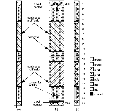
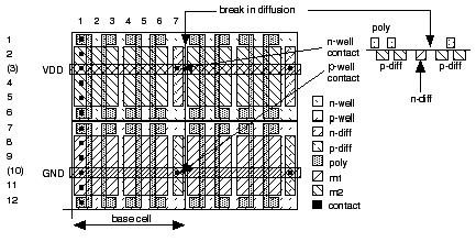
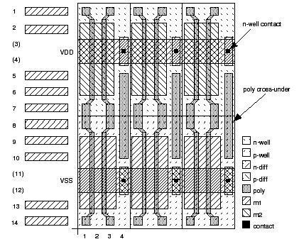
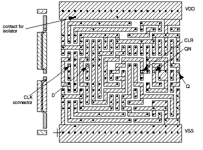
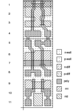
[ Chapter start ] [ Previous page ] [ Next page ] 3.6 Gate-Array DesignEach logic cell or macro in a gate-array library is predesigned using fixed tiles of transistors known as the gate-array base cell (or just base cell ). We call the arrangement of base cells across a whole chip in a complete gate array the gate-array base (or just base ). ASIC vendors offer a selection of bases, with a different total numbers of transistors on each base. For example, if our ASIC design uses 48k equivalent gates and the ASIC vendor offers gate arrays bases with 50k-, 75k-, and 100k-gates, we will probably have to use the 75k-gate base (because it is unlikely that we can use 48/50 or 96 percent of the transistors on the 50k-gate base). We isolate the transistors on a gate array from one another either with thick field oxide (in the case of oxide-isolated gate arrays) or by using other transistors that are wired permanently off (in gate-isolated gate arrays). Channeled and channelless gate arrays may use either gate isolation or oxide isolation. Figure 3.14 (a) shows a base cell for a gate-isolated gate array . This base cell has two transistors: one p -channel and one n -channel. When these base cells are placed next to each other, the n -diffusion and p -diffusion layers form continuous strips that run across the entire chip broken only at the poly gates that cross at regularly spaced intervals (Figure 3.14b). The metal interconnect spacing determines the separation of the transistors. The metal spacing is determined by the design rules for the metal and contacts. In Figure 3.14 (c) we have shown all possible locations for a contact in the base cell. There is room for 21 contacts in this cell and thus room for 21 interconnect lines running in a horizontal direction (we use m1 running horizontally). We say that there are 21 horizontal tracks in this cell or that the cell is 21 tracks high. In a similar fashion the space that we need for a vertical interconnect (m2) is called a vertical track . The horizontal and vertical track widths are not necessarily equal, because the design rules for m1 and m2 are not always equal. We isolate logic cells from each other in gate-isolated gate arrays by connecting transistor gates to the supply bus—hence the name, gate isolation . If we connect the gate of an n -channel transistor to V SS , we isolate the regions of n -diffusion on each side of that transistor (we call this an isolator transistor or device, or just isolator). Similarly if we connect the gate of a p -channel transistor to V DD , we isolate adjacent p -diffusion regions. Oxide-isolated gate arrays often contain four transistors in the base cell: the two n -channel transistors share an n -diffusion strip and the two p -channel transistors share a p -diffusion strip. This means that the two n -channel transistors in each base cell are electrically connected in series, as are the p -channel transistors. The base cells are isolated from each other using oxide isolation . During the fabrication process a layer of the thick field oxide is left in place between each base cell and this separates the p -diffusion and n -diffusion regions of adjacent base cells. Figure 3.15 shows an oxide-isolated gate array . This cell contains eight transistors (which occupy six vertical tracks) plus one-half of a single track that contains the well contacts and substrate connections that we can consider to be shared by each base cell. Figure 3.16 shows a base cell in which the gates of the n -channel and p -channel transistors are connected on the polysilicon layer. Connecting the gates in poly saves contacts and a metal interconnect in the center of the cell where interconnect is most congested. The drawback of the preconnected gates is a loss in flexibility in cell design. Implementing memory and logic based on transmission gates will be less efficient using this type of base cell, for example. Figure 3.17 shows the metal personalization for a D flip-flop macro in a gate-isolated gate array using a base cell similar to that shown in Figure 3.14 (a). This macro uses 20 base cells, for a total of 40 transistors, equivalent to 10 gates. The gates of the base cells shown in Figures 3.14 – 3.16 are bent. The bent gate allows contacts to the gates to be placed on the same grid as the contacts to diffusion. The polysilicon gates run in the space between adjacent metal interconnect lines. This saves space and also simplifies the routing software. There are many trade-offs that determine the gate-array base cell height. One factor is the number of wires that can be run horizontally through the base cell. This will determine the capacity of the routing channel formed from an unused row of base cells. The base cell height also determines how easy it is to wire the logic macros since it determines how much space for wiring is available inside the macros. There are other factors that determine the width of the base-cell transistors. The widths of the p -channel and n -channel transistors are slightly different in Figure 3.14 (a). The p -channel transistors are 6 tracks wide and the n -channel transistors are 5 tracks wide. The ratio for this gate-array library is thus approximately 1.2. Most gate-array libraries are approaching a ratio of 1. ASIC designers are using ever-increasing amounts of RAM on gate arrays. It is inefficient to use the normal base cell for a static RAM cell and the size of RAM on an embedded gate array is fixed. As an alternative we can change the design of the base cell. A base cell designed for use as RAM has extra transistors (either four—two n -channel and two p -channel—or two n -channel; usually minimum width) allowing a six-transistor RAM cell to be built using one base cell instead of the two or three that we would normally need. This is one of the advantages of the CBA (cell-based array) base cell shown in Figure 3.18 .
[ Chapter start ] [ Previous page ] [ Next page ] | ||

