|
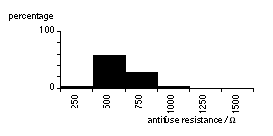
[ Chapter start ] [ Previous page ] [ Next page ] 4.1 The AntifuseAn antifuse is the opposite of a regular fuse—an antifuse is normally an open circuit until you force a programming current through it (about 5 mA). In a poly–diffusion antifuse the high current density causes a large power dissipation in a small area, which melts a thin insulating dielectric between polysilicon and diffusion electrodes and forms a thin (about 20 nm in diameter), permanent, and resistive silicon link . The programming process also drives dopant atoms from the poly and diffusion electrodes into the link, and the final level of doping determines the resistance value of the link. Actel calls its antifuse a programmable low-impedance circuit element ( PLICE ‘ ). Figure 4.1 shows a poly–diffusion antifuse with an oxide–nitride–oxide ( ONO ) dielectric sandwich of: silicon dioxide (SiO 2 ) grown over the n -type antifuse diffusion, a silicon nitride (Si 3 N 4 ) layer, and another thin SiO 2 layer. The layered ONO dielectric results in a tighter spread of blown antifuse resistance values than using a single-oxide dielectric. The effective electrical thickness is equivalent to 10nm of SiO 2 (Si 3 N 4 has a higher dielectric constant than SiO 2 , so the actual thickness is less than 10 nm). Sometimes this device is called a fuse even though it is an anti fuse, and both terms are often used interchangeably. The fabrication process and the programming current control the average resistance of a blown antifuse, but values vary as shown in Figure 4.2 . In a particular technology a programming current of 5 mA may result in an average blown antifuse resistance of about 500 W . Increasing the programming current to 15 mA might reduce the average antifuse resistance to 100 W . Antifuses separate interconnect wires on the FPGA chip and the programmer blows an antifuse to make a permanent connection. Once an antifuse is programmed, the process cannot be reversed. This is an OTP technology (and radiation hard). An Actel 1010, for example, contains 112,000 antifuses (see Table 4.1 ), but we typically only need to program about 2 percent of the fuses on an Actel chip.
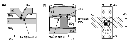
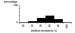
To design and program an Actel FPGA, designers iterate between design entry and simulation. When they are satisfied the design is correct they plug the chip into a socket on a special programming box, called an Activator , that generates the programming voltage. A PC downloads the configuration file to the Activator instructing it to blow the necessary antifuses on the chip. When the chip is programmed it may be removed from the Activator without harming the configuration data and the chip assembled into a system. One disadvantage of this procedure is that modern packages with hundreds of thin metal leads are susceptible to damage when they are inserted and removed from sockets. The advantage of other programming technologies is that chips may be programmed after they have been assembled on a printed-circuit board—a feature known as in-system programming ( ISP ). The Actel antifuse technology uses a modified CMOS process. A double-metal, single-poly CMOS process typically uses about 12 masks—the Actel process requires an additional three masks. The n- type antifuse diffusion and antifuse polysilicon require an extra two masks and a 40 nm (thicker than normal) gate oxide (for the high-voltage transistors that handle 18 V to program the antifuses) uses one more masking step. Actel and Data General performed the initial experiments to develop the PLICE technology and Actel has licensed the technology to Texas Instruments (TI). The programming time for an ACT 1 device is 5 to 10 minutes. Improvements in programming make the programming time for the ACT 2 and ACT 3 devices about the same as the ACT 1. A 5-day work week, with 8-hour days, contains about 2400 minutes. This is enough time to program 240 to 480 Actel parts per week with 100 percent efficiency and no hardware down time. A production schedule of more than 1000 parts per month requires multiple or gang programmers. 4.1.1 Metal–Metal AntifuseFigure 4.3 shows a QuickLogic metal–metal antifuse ( ViaLink ‘ ). The link is an alloy of tungsten, titanium, and silicon with a bulk resistance of about 500 mW cm. There are two advantages of a metal–metal antifuse over a poly–diffusion antifuse. The first is that connections to a metal–metal antifuse are direct to metal—the wiring layers. Connections from a poly–diffusion antifuse to the wiring layers require extra space and create additional parasitic capacitance. The second advantage is that the direct connection to the low-resistance metal layers makes it easier to use larger programming currents to reduce the antifuse resistance. For example, the antifuse resistance R ⊕ 0.8/ I , with the programming current I in mA and R in W , for the QuickLogic antifuse. Figure 4.4 shows that the average QuickLogic metal–metal antifuse resistance is approximately 80 W (with a standard deviation of about 10 W ) using a programming current of 15 mA as opposed to an average antifuse resistance of 500 W (with a programming current of 5 mA) for a poly–diffusion antifuse.
The size of an antifuse is limited by the resolution of the lithography equipment used to makes ICs. The Actel antifuse connects diffusion and polysilicon, and both these materials are too resistive for use as signal interconnects. To connect the antifuse to the metal layers requires contacts that take up more space than the antifuse itself, reducing the advantage of the small antifuse size. However, the antifuse is so small that it is normally the contact and metal spacing design rules that limit how closely the antifuses may be packed rather than the size of the antifuse itself. An antifuse is resistive and the addition of contacts adds parasitic capacitance. The intrinsic parasitic capacitance of an antifuse is small (approximately 1–2 fF in a 1 m m CMOS process), but to this we must add the extrinsic parasitic capacitance that includes the capacitance of the diffusion and poly electrodes (in a poly–diffusion antifuse) and connecting metal wires (approximately 10 fF). These unwanted parasitic elements can add considerable RC interconnect delay if the number of antifuses connected in series is not kept to an absolute minimum. Clever routing techniques are therefore crucial to antifuse-based FPGAs. The long-term reliability of antifuses is an important issue since there is a tendency for the antifuse properties to change over time. There have been some problems in this area, but as a result we now know an enormous amount about this failure mechanism. There are many failure mechanisms in ICs—electromigration is a classic example—and engineers have learned to deal with these problems. Engineers design the circuits to keep the failure rate below acceptable limits and systems designers accept the statistics. All the FPGA vendors that use antifuse technology have extensive information on long-term reliability in their data books. [ Chapter start ] [ Previous page ] [ Next page ] | |||||||||||||||||||||||||||||||


