


Supports High-Speed and High-Accuracy Banknote Recognition Applications for Chinese Market
TOKYO — (BUSINESS WIRE) — July 25, 2013 — Toshiba Corporation (TOKYO:6502) announced today that the launch of "CIPS183BS210", a Contact Image-Sensor Module with a faster data rate, for application in banknote recognition systems. Mass production is scheduled to start in October 2013.
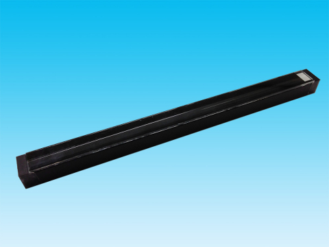
Toshiba Contact Image-Sensor Module for Banknote Recognition (Photo: Business Wire)
"CIPS183BS210" incorporates a newly developed linear image sensor and offers a 16MHz data rate, twice that of its predecessor, the CIPS183BS200. It realizes the same rate of banknote recognition in high resolution mode (200dpi) as the current product does in high speed mode (100dpi). This improvement realizes the high-accuracy and high-speed banknote recognition required for application in the Chinese market.
The new module is 14mm wide against 18mm for the current generation of product, and also offers improved luminous intensity distribution.
Customized module cases will be considered as an option, at the request of customers.
Applications
Banknote recognition systems, such as counting and
sorting machines, automated teller machines (ATM), etc
Key features
1. Integration of newly developed high-speed,
high-sensitivity linear sensor enables:
- High speed data rate of 16MHz
-
High sensitivity
- RGB sensitivity is improved by approximately 70% (Comparison with CIPS183BS200)
- Infrared sensitivity is improved by approximately 25% (Comparison with CIPS183BS200)
- Stable output signals, securing operation margin and simplifying system design
2. Module width is reduced to 14mm.
|
Main Specifications |
||
| Product Name | CIPS183BS210 | |
| Effective Scanning Length | 183 mm | |
| Resolution | 200dpi / 100dpi (selectable) | |
| Light Source | R/G/B/IR | |
| Scanning Speed |
41µs x 4 /line (at 200dpi)
23µs x 4 /line (at 100dpi) |
|
| Data rate | 16MHz | |
| Module dimension | 200(L) x 14(W) x 12.4(H) mm | |
| Sample schedule | August, 2013 | |
| Mass production schedule | October, 2013 | |


 Animation, 3D Art and 3D Models")