


Incorporating Two Kinds of Communication Functions for Wearable Healthcare Low Power Devices
TOKYO — (BUSINESS WIRE) — September 24, 2014 — Toshiba Corporation (TOKYO:6502) today announced the launch of “TC35670FTG”, a low power consumption dual function IC that supports both Bluetooth® Low Energy (LE)[1] communications and NFC Type 3 Tag. Sample shipments start today.
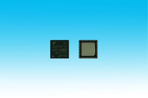
Toshiba launches low power consumption ICs "TC35670FTG" for Bluetooth(R) Smart communication devices with NFC Tag functions (Photo: Business Wire)
Recently, more and more Bluetooth® Smart[2] devices offer Bluetooth® LE compatibility. The new IC joins Toshiba’s line-up of Bluetooth® LE ICs, and offer two key features: easy operation of Bluetooth® pairing with NFC Tag function; long-time stand-by status for devices powered by small coin-cell batteries. The IC will facilitate adoption of Bluetooth® LE communications in small devices, such as wearable healthcare devices, sensors, toys and, most notably, future touch and start smartphone accessories.
Previously, set makers had to integrate ICs for both Bluetooth® and NFC Tag when designing a system supporting both communication functions. Toshiba’s new approach offers a design that will help to minimize the part counts, reduce the assembly area by about 30% and shorten system development.
The NFC Tag component has a 1.5 Kbyte E2PROM for storing data that set makers can access using both the Bluetooth® LE and NFC Tag to connect each I2C interfaces, allowing data to be easily handled in each system.
| These functionalities allow the new device to support three ways of use: | ||
| 1. |
Put both Bluetooth® LE and NFC Tag in stand-by mode and prioritize the connection from the 1st access. |
|
| 2. | By adding NFC Tag function, easy pairing of Bluetooth® LE devices can be realized and a long time stand-by status can be maintained. | |
| 3. | The NFC Tag can provide a system on/off switch function, and cut off the hardware switch from a lot of devices that are required to reduce stand-by power. | |
Key Features of the New Product
-
Low power consumption:
- Below 5.9mA at peak consumption of Bluetooth® communication (@3.3V, -4dBm transmitter output power or receiver operation)
- Below 600μA for NFC Tag communication (@3.3V)
- Below 0.5μA in deep sleep (@3.3V)[3]
- Receiver sensitivity: -92.5dBm
- Supports Bluetooth® LE central and peripheral devices
- Supports servers and client functions defined by GATT (Generic Attribute Profile)
- NFC Forum Type 3 Tag


 Animation, 3D Art and 3D Models")