- Utilizing Novel Split-Gate Technology to Boost Bit Density -
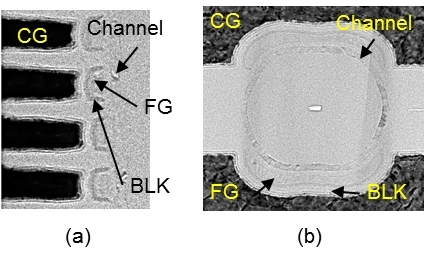
TOKYO — (BUSINESS WIRE) — December 11, 2019 — Kioxia Corporation today announced the development of the world’s first[1] three-dimensional (3D) semicircular split-gate flash memory cell structure “Twin BiCS FLASH” using specially designed semicircular Floating Gate (FG) cells. Twin BiCS FLASH achieves superior program slope and a larger program/erase window at a much smaller cell size compared to conventional circular Charge Trap (CT) cells. These attributes make this new cell design a promising candidate to surpass four bits per cell (QLC) for significantly higher memory density and fewer stacking layers. This technology was announced at the IEEE International Electron Devices Meeting (IEDM) held in San Francisco, CA on December 11th.
This press release features multimedia. View the full release here: https://www.businesswire.com/news/home/20191211006038/en/

Fabricated semicircular FG cells (a) Cross-sectional view (b) Plane view (Graphic: Business Wire)
3D flash memory technology has achieved high bit density with low cost per bit by increasing the number of cell stacked layers as well as by implementing multilayer stack deposition and high aspect ratio etching. In recent years, as the number of cell layers exceeds 100, managing the trade-offs among etch profile control, size uniformity and productivity is becoming increasingly challenging. To overcome this problem, Kioxia developed a new semicircular cell design by splitting the gate electrode in the conventional circular cell to reduce cell size compared to the conventional circular cell, enabling higher-density memory at a lower number of cell layers.
The circular control gate provides a larger program window with relaxed saturation problems when compared with a planar gate because of the curvature effect, where carrier injection through the tunnel dielectric is enhanced while electron leakage to the block (BLK) dielectric is lowered. In this split-gate cell design, the circular control gate is symmetrically divided into two semicircular gates to take advantage of the strong improvement in the program/erase dynamics. As shown in Fig. 1, the conductive storage layer is employed for high charge trapping efficiency in conjunction with the high-k BLK dielectrics, achieving high coupling ratio to gain program window as well as reduced electron leakage from the FG, thus relieving the saturation issue. The experimental program/erase characteristics in Fig. 2 reveal that the semicircular FG cells with the high-k-based BLK exhibit significant gains in the program slope and program/erase window over the larger-sized circular CT cells. The semicircular FG cells, having superior program/erase characteristics, are expected to attain comparably tight QLC Vt distributions at small cell size. Further, integration of low-trap Si channel makes possible more than four bits/cell, e.g., Penta-Level Cell (PLC) as shown in Fig. 3. These results confirm that semicircular FG cells are a viable option to pursue higher bit density.
Going forward, Kioxia’s research and development efforts aimed at innovation in flash memory will include continuing Twin BiCS FLASH development and seeking its practical applications. At IEDM 2019, Kioxia also announced six other papers highlighting the company’s intensive R&D activities in the area of flash memory.
[1] Source: Kioxia Corporation, as of December 12, 2019.
About Kioxia
Kioxia is a world leader in memory solutions, dedicated to the development, production and sale of flash memory and solid state drives (SSDs). In April 2017, its predecessor Toshiba Memory was spun off from Toshiba Corporation, the company that invented NAND flash memory in 1987. Kioxia is committed to uplifting the world with memory by offering products, services and systems that create choice for customers and memory-based value for society. Kioxia's innovative 3D flash memory technology, BiCS FLASH™, is shaping the future of storage in high-density applications, including advanced smartphones, PCs, SSDs, automotive and data centers.
View source version on businesswire.com: https://www.businesswire.com/news/home/20191211006038/en/
Contact:
Kioxia Holdings Corporation
Kota Yamaji
Public Relations
Phone: +81-3-6478-2319
kioxia-hd-pr@kioxia.com


