EUV-based 1st-gen 10nm-class DRAM (D1x) has completed its customer evaluations;
EUV to be fully deployed from 4th-gen 10nm-class DRAM (D1a) next year
SEOUL, South Korea — (BUSINESS WIRE) — March 25, 2020 — Samsung Electronics Co., Ltd., the world leader in advanced memory technology, today announced that it has successfully shipped one million of the industry's first 10nm-class (D1x) DDR4 (Double Date Rate 4) DRAM modules based on extreme ultraviolet (EUV) technology. The new EUV-based DRAM modules have completed global customer evaluations, and will open the door to more cutting-edge EUV process nodes for use in premium PC, mobile, enterprise server and datacenter applications.
This press release features multimedia. View the full release here: https://www.businesswire.com/news/home/20200325005238/en/

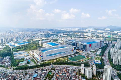
Samsung Electronics Hwaseong Campus (Photo: Business Wire)
"With the production of our new EUV-based DRAM, we are demonstrating our full commitment toward providing revolutionary DRAM solutions in support of our global IT customers,” said Jung-bae Lee, executive vice president of DRAM Product & Technology at Samsung Electronics. "This major advancement underscores how we will continue contributing to global IT innovation through timely development of leading-edge process technologies and next-generation memory products for the premium memory market."
Samsung is the first to adopt EUV in DRAM production to overcome challenges in DRAM scaling. EUV technology reduces repetitive steps in multi-patterning and improves patterning accuracy, enabling enhanced performance and greater yields as well as shortened development time.
EUV will be fully deployed in Samsung's future generations of DRAM, starting with its fourth-generation 10nm-class (D1a) or the highly-advanced 14nm-class, DRAM. Samsung expects to begin volume production of D1a-based DDR5 and LPDDR5 next year, which would double manufacturing productivity of the 12-inch D1x wafers.
In line with the expansion of the DDR5/LPDDR5 market next year, the company will further strengthen its collaboration with leading IT customers and semiconductor vendors on optimizing standard specifications, as it accelerates the transition to DDR5/LPDDR5 throughout the memory market.
To better address the growing demand for next-generation premium DRAM, Samsung will start the operation of a second semiconductor fabrication line in Pyeongtaek, South Korea, within the second half of this year.
Timeline of Samsung DRAM Milestones
Date |
Samsung DRAM Milestones |
2021 (TBD) |
4th-gen 10nm-class (1a) EUV-based 16Gb DDR5/LPDDR5 mass production |
March 2020 |
4th-gen 10nm-class (1a) EUV-based DRAM development |
September 2019 |
3rd-gen 10nm-class (1z) 8Gb DDR4 mass production |
June 2019 |
2nd-gen 10nm-class (1y) 12Gb LPDDR5 mass production |
March 2019 |
3rd-gen 10nm-class (1z) 8Gb DDR4 development |
November 2017 |
2nd-gen 10nm-class (1y) 8Gb DDR4 mass production |
September 2016 |
1st-gen 10nm-class (1x) 16Gb LPDDR4/4X mass production |
February 2016 |
1st-gen 10nm-class (1x) 8Gb DDR4 mass production |
October 2015 |
20nm (2z) 12Gb LPDDR4 mass production |
December 2014 |
20nm (2z) 8Gb GDDR5 mass production |
December 2014 |
20nm (2z) 8Gb LPDDR4 mass production |
October 2014 |
20nm (2z) 8Gb DDR4 mass production |
February 2014 |
20nm (2z) 4Gb DDR3 mass production |
February 2014 |
20nm-class (2y) 8Gb LPDDR4 mass production |
November 2013 |
20nm-class (2y) 6Gb LPDDR3 mass production |
November 2012 |
20nm-class (2y) 4Gb DDR3 mass production |
September 2011 |
20nm-class (2x) 2Gb DDR3 mass production |
July 2010 |
30nm-class 2Gb DDR3 mass production |
February 2010 |
40nm-class 4Gb DDR3 mass production |
July 2009 |
40nm-class 2Gb DDR3 mass production |
###
About Samsung Electronics Co., Ltd.
Samsung inspires the world and shapes the future with transformative ideas and technologies. The company is redefining the worlds of TVs, smartphones, wearable devices, tablets, digital appliances, network systems, and memory, system LSI, foundry and LED solutions. For the latest news, please visit the Samsung Newsroom at http://news.samsung.com.
View source version on businesswire.com: https://www.businesswire.com/news/home/20200325005238/en/
Contact:
Ujeong Jahnke
Samsung Semiconductor Europe GmbH
Tel. +49(0)6196-66-3300
Email:
ujeong.j@samsung.com


