Ansys' new breakthrough technology helps engineers improve product design for advanced applications ranging from autonomous vehicles to 5G communications
PITTSBURGH, Jan. 21, 2021 — (PRNewswire) —/ Key Highlights
- Ansys is empowering engineers to mesh and solve bigger designs than ever thought possible with the launch of Ansys HFSS Mesh Fusion
- Slashing development costs and spurring the creation of next-generation products, HFSS Mesh Fusion powers fast and fully-coupled simulation of complex electromagnetic (EM) systems — without compromise to the design or fidelity
Ansys (NASDAQ: ANSS) is helping engineering teams to mesh and solve larger designs than ever with the launch of Ansys HFSS Mesh Fusion. Cutting development expenses and expediting the development of leading-edge products, HFSS Mesh Fusion drives rapid and fully coupled simulation of complex EM systems — without compromising the design or fidelity.
Modern electronic products are more sophisticated than ever, with higher density, lower voltage margins and more advanced processes. To deliver innovation, engineers must increase functionality and maintain or even decrease power consumption within a smaller form factor. As these designs become more challenging, engineers must solve complex interactions between components and across systems, critical for designing cutting-edge artificial intelligence machine learning, autonomous vehicle, 5G communications, high-performance computing and Industrial Internet of Things applications.
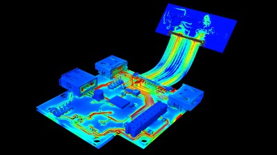
HFSS Mesh Fusion, available in Ansys HFSS 2021 R1, helps engineers combine integrated circuits (IC), packaging, connectors, printed circuit boards, antennas and platform in a single Ansys HFSS analysis to predict EM interactions. HFSS Mesh Fusion bypasses previous barriers by applying optimal meshing technology at the component level, parallelized across cores, clusters or within Ansys® Cloud™. A breakthrough solver technology then extracts a fully coupled, uncompromised, full-wave EM matrix. By enabling much more complex designs to be solved, companies can confidently push the limits of performance to create state-of-the-art products.
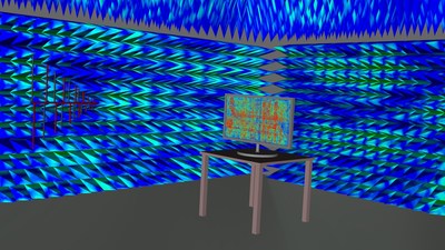
"Increasing levels of electronic system integration are leading to a greater demand for comprehensive EM system analysis," said Sangyun Kim, vice president, Foundry Design Technology Team at Samsung Electronics. "Ansys HFSS Mesh Fusion makes it possible for our talented engineering teams to create optimal designs, shrink design cycles and cost and increase the value that we deliver to our customers. Leveraging Mesh Fusion, we are innovating highly advanced designs that were previously unimaginable. In fact, for the customer's latest flat panel TV, we simulated the EM transmission of an entire room."
HFSS Mesh Fusion helps engineers swiftly overcome the most challenging design obstacles to deliver best-in-class products to customers.
"Ansys HFSS can solve any structure, regardless of complexity, enabling creative out-of-the-box designs. The new HFSS Mesh Fusion technology will allow us to tackle even more comprehensive, uncompromised simulations with HFSS, further validating it as our 'virtual laboratory'," said Clyde Callewaert, senior engineer at Herrick Technology Labs. "Because with HFSS in the loop, we go into the lab to confirm results, not discover them."
By solving the most complex EM models, HFSS Mesh Fusion delivers critical design data that improves end products.
"HFSS Mesh Fusion helps IC designers effectively manage the capacity, complexity, dimensional range and density of geometric detail in a fully coupled EM simulation," said John Lee, vice president and general manager at Ansys. "This empowers engineers to break the old rules, innovate leading-edge designs at higher frequencies and within tighter form factors, tape out with confidence and deliver trailblazing products with more functionality than ever thought possible. This supports numerous highly sophisticated applications, including 5G communications, autonomous driving and many more."
/ About Ansys
If you've ever seen a rocket launch, flown on an airplane, driven a car, used a computer, touched a mobile device, crossed a bridge or put on wearable technology, chances are you've used a product where Ansys software played a critical role in its creation. Ansys is the global leader in engineering simulation. Through our strategy of Pervasive Engineering Simulation, we help the world's most innovative companies deliver radically better products to their customers. By offering the best and broadest portfolio of engineering simulation software, we help them solve the most complex design challenges and create products limited only by imagination. Founded in 1970, Ansys is headquartered south of Pittsburgh, Pennsylvania, U.S.A. Visit www.ansys.com for more information.
Ansys and any and all ANSYS, Inc. brand, product, service and feature names, logos and slogans are registered trademarks or trademarks of ANSYS, Inc. or its subsidiaries in the United States or other countries. All other brand, product, service and feature names or trademarks are the property of their respective owners.
ANSS–T
/ Contacts
Media | Mary Kate Joyce |
|
| 724.820.4368 |
|
| marykate.joyce@ansys.com |
| Annette N. Arribas, IRC |
|
| 724.820.3700 |
|
| annette.arribas@ansys.com |
![]() View original content to download multimedia:
http://www.prnewswire.com/news-releases/ansys-launches-hfss-mesh-fusion-redefines-product-development-by-enabling-design-of-entire-systems-301211969.html
View original content to download multimedia:
http://www.prnewswire.com/news-releases/ansys-launches-hfss-mesh-fusion-redefines-product-development-by-enabling-design-of-entire-systems-301211969.html
SOURCE Ansys
| Contact: |
| Company Name: Ansys
Web: https://www.ansys.com Financial data for Ansys |


