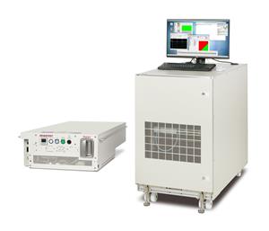
TOKYO, Nov. 29, 2021 (GLOBE NEWSWIRE) -- Leading semiconductor test equipment supplier Advantest Corporation (TSE: 6857) has introduced a new high-throughput memory tester for NAND flash devices that can perform functional testing of chips while delivering highly accurate timing, repeatability and failure detection. With data-transfer speeds that are more than five times faster than its predecessor, the new T5221 system is designed to improve production efficiencies while reducing test costs for wafer sorting, built-in self-testing (BIST) and wafer-level burn-in (WLBI).
Worldwide sales of NAND wafer test equipment for multi-stacked type probers are approximately US$100 million per year, accounting for an estimated seven percent of the total memory market. As the market grows, customers are shifting away from high-functionality wafer-sorting test equipment toward more cost-effective design-for-test (DFT) and BIST strategies using multi-probe systems.
The T5221 is optimized for use with a multi-wafer prober. The system controller can simultaneously manage up to 12 test stations, each with independent testing capabilities. The combined-array architecture reduces test times while the tester’s massive parallelism allows it to perform wafer-level testing on up to 1,152 devices at once.
The system’s test stations do not add to the overall footprint because they are housed within the multi-wafer prober. This allows the T5221 platform to use much less floor space than Advantest’s previous nonvolatile memory tester and a standalone prober.
The new tester can be docked with either a 12-stage multi-wafer prober for use in mass production or single- or dual-wafer probers in engineering environments.
Probe card design has been simplified to lower both the cost of ownership and cost of test. The unit incorporates a combined performance board that eliminates the need for a printed circuit board on the probe card.
System features include two driver pins and one I/O pin for each device under test as well as a flexible algorithmic pattern generator (ALPG), a waveform generator and various self-diagnostic functions.
To further enhance the T5221’s performance range, an optional upgrade is available to boost the power-supply level as high as 28 volts while still measuring small currents down to one nanoampere (nA). These capabilities are not available in many competitive products.
There is even a “green” element to the new tester. The environmentally friendly design eliminates the use of toxic substances in separating and disassembling the system’s parts.
The T5221’s operation is fully compatible with Advantest’s legacy memory solutions to provide users with a seamless transition from previous generations of equipment.
“The launch of our T5221 platform fits with Advantest’s strategy to offer new advantages in the NAND wafer-level test market,” said Masayuki Suzuki, executive vice president of the Memory Test Business Unit for Advantest Corporation. “With this system’s advanced performance hardware and high-speed data-transfer capabilities, we can significantly reduce test time and costs compared to competitive products.”
T5221 testers are expected to begin shipping to customers by the first quarter of 2022.
About Advantest Corporation
Advantest (TSE: 6857) is the leading manufacturer of automatic test and measurement equipment used in the design and production of semiconductors for applications including 5G communications, the Internet of Things (IoT), autonomous vehicles, artificial intelligence (AI), machine learning, smart medical devices and more. Its leading-edge systems and products are integrated into the most advanced semiconductor production lines in the world. The company also conducts R&D to address emerging testing challenges and applications, produces multi-vision metrology scanning electron microscopes essential to photomask manufacturing, and offers groundbreaking 3D imaging and analysis tools. Founded in Tokyo in 1954, Advantest is a global company with facilities around the world and an international commitment to sustainable practices and social responsibility. More information is available at
www.advantest.com.
ADVANTEST CORPORATION
3061 Zanker Road
San Jose, CA 95134, USA
Amy Gold
amy.gold@advantest.com
A photo accompanying this announcement is available at https://www.globenewswire.com/NewsRoom/AttachmentNg/42860728-ace2-492a-96d9-3d8b2d77a227


