|
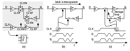
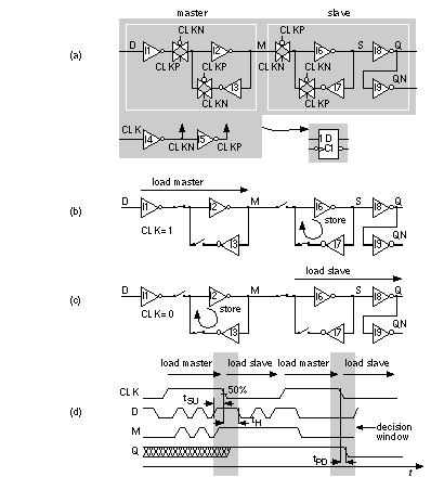
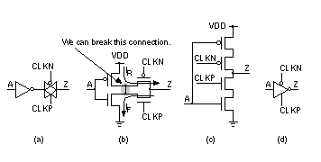
[ Chapter start ] [ Previous page ] [ Next page ] 2.5 Sequential Logic CellsThere are two main approaches to clocking in VLSI design: multiphase clocks or a single clock and synchronous design . The second approach has the following key advantages: (1) it allows automated design, (2) it is safe, and (3) it permits vendor signoff (a guarantee that the ASIC will work as simulated). These advantages of synchronous design (especially the last one) usually outweigh every other consideration in the choice of a clocking scheme. The vast majority of ASICs use a rigid synchronous design style. 2.5.1 LatchFigure 2.17(a) shows a sequential logic cell—a latch . The internal clock signals, CLKN (N for negative) and CLKP (P for positive), are generated from the system clock, CLK, by two inverters (I4 and I5) that are part of every latch cell—it is usually too dangerous to have these signals supplied externally, even though it would save space. To emphasize the difference between a latch and flip-flop, sometimes people refer to the clock input of a latch as an enable . This makes sense when we look at Figure 2.17(b), which shows the operation of a latch. When the clock input is high, the latch is transparent —changes at the D input appear at the output Q (quite different from a flip-flop as we shall see). When the enable (clock) goes low (Figure 2.17c), inverters I2 and I3 are connected together, forming a storage loop that holds the last value on D until the enable goes high again. The storage loop will hold its state as long as power is on; we call this a static latch. A sequential logic cell is different from a combinational cell because it has this feature of storage or memory. Notice that the output Q is unbuffered and connected directly to the output of I2 (and the input of I3), which is a storage node. In an ASIC library we are conservative and add an inverter to buffer the output, isolate the sensitive storage node, and thus invert the sense of Q. If we want both Q and QN we have to add two inverters to the circuit of Figure 2.17(a). This means that a latch requires seven inverters and two TGs (4.5 gates). The latch of Figure 2.17(a) is a positive-enable D latch, active-high D latch, or transparent-high D latch (sometimes people also call this a D-type latch). A negative-enable (active-low) D latch can be built by inverting all the clock polarities in Figure 2.17(a) (swap CLKN for CLKP and vice-versa). 2.5.2 Flip-FlopFigure 2.18(a) shows a flip-flop constructed from two D latches: a master latch (the first one) and a slave latch . This flip-flop contains a total of nine inverters and four TGs, or 6.5 gates. In this flip-flop design the storage node S is buffered and the clock-to-Q delay will be one inverter delay less than the clock-to-QN delay. In Figure 2.18(b) the clock input is high, the master latch is transparent, and node M (for master) will follow the D input. Meanwhile the slave latch is disconnected from the master latch and is storing whatever the previous value of Q was. As the clock goes low (the negative edge) the slave latch is enabled and will update its state (and the output Q) to the value of node M at the negative edge of the clock. The slave latch will then keep this value of M at the output Q, despite any changes at the D input while the clock is low (Figure 2.18c). When the clock goes high again, the slave latch will store the captured value of M (and we are back where we started our explanation). The combination of the master and slave latches acts to capture or sample the D input at the negative clock edge, the active clock edge . This type of flip-flop is a negative-edge–triggered flip-flop and its behavior is quite different from a latch. The behavior is shown on the IEEE symbol by using a triangular “notch” to denote an edge-sensitive input. A bubble shows the input is sensitive to the negative edge. To build a positive-edge–triggered flip-flop we invert the polarity of all the clocks—as we did for a latch. The waveforms in Figure 2.18(d) show the operation of the flip-flop as we have described it, and illustrate the definition of setup time ( t SU ), hold time ( t H ), and clock-to-Q propagation delay ( t PD ). We must keep the data stable (a fixed logic '1' or '0') for a time t SU prior to the active clock edge, and stable for a time t H after the active clock edge (during the decision window shown). In Figure 2.18(d) times are measured from the points at which the waveforms cross 50 percent of V DD . We say the trip point is 50 percent or 0.5. Common choices are 0.5 or 0.65/0.35 (a signal has to reach 0.65 V DD to be a '1', and reach 0.35 V DD to be a '0'), or 0.1/0.9 (there is no standard way to write a trip point). Some vendors use different trip points for the input and output waveforms (especially in I/O cells). The flip-flop in Figure 2.18(a) is a D flip-flop and is by far the most widely used type of flip-flop in ASIC design. There are other types of flip-flops—J-K, T (toggle), and S-R flip-flops—that are provided in some ASIC cell libraries mainly for compatibility with TTL design. Some people use the term register to mean an array (more than one) of flip-flops or latches (on a data bus, for example), but some people use register to mean a single flip-flop or a latch. This is confusing since flip-flops and latches are quite different in their behavior. When I am talking about logic cells, I use the term register to mean more than one flip-flop. To add an asynchronous set (Q to '1') or asynchronous reset (Q to '0') to the flip-flop of Figure 2.18(a), we replace one inverter in both the master and slave latches with two-input NAND cells. Thus, for an active-low set, we replace I2 and I7 with two-input NAND cells, and, for an active-low reset, we replace I3 and I6. For both set and reset we replace all four inverters: I2, I3, I6, and I7. Some TTL flip-flops have dominant reset or dominant set , but this is difficult (and dangerous) to do in ASIC design. An input that forces Q to '1' is sometimes also called preset . The IEEE logic symbols use 'P' to denote an input with a presetting action. An input that forces Q to '0' is often also called clear . The IEEE symbols use 'R' to denote an input with a resetting action. 2.5.3 Clocked InverterFigure 2.19 shows how we can derive the structure of a clocked inverter from the series combination of an inverter and a TG. The arrows in Figure 2.19(b) represent the flow of current when the inverter is charging ( I R ) or discharging ( I F ) a load capacitance through the TG. We can break the connection between the inverter cells and use the circuit of Figure 2.19(c) without substantially affecting the operation of the circuit. The symbol for the clocked inverter shown in Figure 2.19(d) is common, but by no means a standard. We can use the clocked inverter to replace the inverter–TG pairs in latches and flip-flops. For example, we can replace one or both of the inverters I1 and I3 (together with the TGs that follow them) in Figure 2.17(a) by clocked inverters. There is not much to choose between the different implementations in this case, except that layout may be easier for the clocked inverter versions (since there is one less connection to make). More interesting is the flip-flop design: We can only replace inverters I1, I3, and I7 (and the TGs that follow them) in Figure 2.18(a) by clocked inverters. We cannot replace inverter I6 because it is not directly connected to a TG. We can replace the TG attached to node M with a clocked inverter, and this will invert the sense of the output Q, which thus becomes QN. Now the clock-to-Q delay will be slower than clock-to-QN, since Q (which was QN) now comes one inverter later than QN. If we wish to build a flip-flop with a fast clock-to-QN delay it may be better to build it using clocked inverters and use inverters with TGs for a flip-flop with a fast clock-to-Q delay. In fact, since we do not always use both Q and QN outputs of a flip-flop, some libraries include Q only or QN only flip-flops that are slightly smaller than those with both polarity outputs. It is slightly easier to layout clocked inverters than an inverter plus a TG, so flip-flops in commercial libraries include a mixture of clocked-inverter and TG implementations. [ Chapter start ] [ Previous page ] [ Next page ] | |


