|
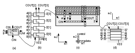
[ Chapter start ] [ Previous page ] [ Next page ] 2.6 Datapath Logic CellsSuppose we wish to build an n -bit adder (that adds two n -bit numbers) and to exploit the regularity of this function in the layout. We can do so using a datapath structure. The following two functions, SUM and COUT, implement the sum and carry out for a full adder ( FA ) with two data inputs (A, B) and a carry in, CIN: The sum uses the parity function ('1' if there are an odd numbers of '1's in the inputs). The carry out, COUT, uses the 2-of-3 majority function ('1' if the majority of the inputs are '1'). We can combine these two functions in a single FA logic cell, ADD(A[ i ], B[ i ], CIN, S[ i ], COUT), shown in Figure 2.20(a), where Now we can build a 4-bit ripple-carry adder ( RCA ) by connecting four of these ADD cells together as shown in Figure 2.20(b). The i th ADD cell is arranged with the following: two bus inputs A[ i ], B[ i ]; one bus output S[ i ]; an input, CIN, that is the carry in from stage ( i – 1) below and is also passed up to the cell above as an output; and an output, COUT, that is the carry out to stage ( i + 1) above. In the 4-bit adder shown in Figure 2.20(b) we connect the carry input, CIN[0], to VSS and use COUT[3] and COUT[2] to indicate arithmetic overflow (in Section 2.6.1 we shall see why we may need both signals). Notice that we build the ADD cell so that COUT[2] is available at the top of the datapath when we need it. Figure 2.20(c) shows a layout of the ADD cell. The A inputs, B inputs, and S outputs all use m1 interconnect running in the horizontal direction—we call these data signals. Other signals can enter or exit from the top or bottom and run vertically across the datapath in m2—we call these control signals. We can also use m1 for control and m2 for data, but we normally do not mix these approaches in the same structure. Control signals are typically clocks and other signals common to elements. For example, in Figure 2.20(c) the carry signals, CIN and COUT, run vertically in m2 between cells. To build a 4-bit adder we stack four ADD cells creating the array structure shown in Figure 2.20(d). In this case the A and B data bus inputs enter from the left and bus S, the sum, exits at the right, but we can connect A, B, and S to either side if we want. The layout of buswide logic that operates on data signals in this fashion is called a datapath . The module ADD is a datapath cell or datapath element . Just as we do for standard cells we make all the datapath cells in a library the same height so we can abut other datapath cells on either side of the adder to create a more complex datapath. When people talk about a datapath they always assume that it is oriented so that increasing the size in bits makes the datapath grow in height, upwards in the vertical direction, and adding different datapath elements to increase the function makes the datapath grow in width, in the horizontal direction—but we can rotate and position a completed datapath in any direction we want on a chip. What is the difference between using a datapath, standard cells, or gate arrays? Cells are placed together in rows on a CBIC or an MGA, but there is no generally no regularity to the arrangement of the cells within the rows—we let software arrange the cells and complete the interconnect. Datapath layout automatically takes care of most of the interconnect between the cells with the following advantages:
There are some disadvantages of using a datapath:
There are some newer standard-cell and gate-array tools that can take advantage of regularity in a design and position cells carefully. The problem is in finding the regularity if it is not specified. Using a datapath is one way to specify regularity to ASIC design tools. 2.6.1 Datapath ElementsFigure 2.21 shows some typical datapath symbols for an adder (people rarely use the IEEE standards in ASIC datapath libraries). I use heavy lines (they are 1.5 point wide) with a stroke to denote a data bus (that flows in the horizontal direction in a datapath), and regular lines (0.5 point) to denote the control signals (that flow vertically in a datapath). At the risk of adding confusion where there is none, this stroke to indicate a data bus has nothing to do with mixed-logic conventions. For a bus, A[31:0] denotes a 32-bit bus with A[31] as the leftmost or most-significant bit or MSB , and A[0] as the least-significant bit or LSB . Sometimes we shall use A[MSB] or A[LSB] to refer to these bits. Notice that if we have an n -bit bus and LSB = 0, then MSB = n – 1. Also, for example, A[4] is the fifth bit on the bus (from the LSB). We use a ' S ' or 'ADD' inside the symbol to denote an adder instead of '+', so we can attach '–' or '+/–' to the inputs for a subtracter or adder/subtracter. Some schematic datapath symbols include only data signals and omit the control signals—but we must not forget them. In Figure 2.21, for example, we may need to explicitly tie CIN[0] to VSS and use COUT[MSB] and COUT[MSB – 1] to detect overflow. Why might we need both of these control signals? Table 2.11 shows the process of simple arithmetic for the different binary number representations, including unsigned, signed magnitude, ones’ complement, and two’s complement.
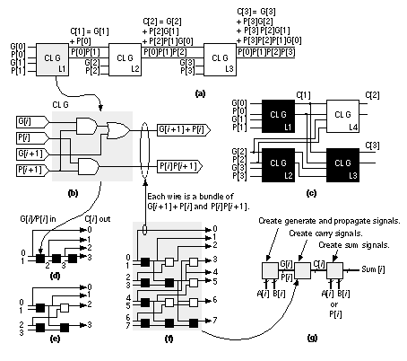
2.6.2 AddersWe can view addition in terms of generate , G[ i ], and propagate , P[ i ], signals. where C[ i ] is the carry-out signal from stage i , equal to the carry in of stage ( i + 1). Thus, C[ i ] = COUT[ i ] = CIN[ i + 1]. We need to be careful because C[0] might represent either the carry in or the carry out of the LSB stage. For an adder we set the carry in to the first stage (stage zero), C[–1] or CIN[0], to '0'. Some people use delete (D) or kill (K) in various ways for the complements of G[i] and P[i], but unfortunately others use C for COUT and D for CIN—so I avoid using any of these. Do not confuse the two different methods (both of which are used) in Eqs. 2.42–2.45 when forming the sum, since the propagate signal, P[ i ] , is different for each method. Figure 2.22(a) shows a conventional RCA. The delay of an n -bit RCA is proportional to n and is limited by the propagation of the carry signal through all of the stages. We can reduce delay by using pairs of “go-faster” bubbles to change AND and OR gates to fast two-input NAND gates as shown in Figure 2.22(a). Alternatively, we can write the equations for the carry signal in two different ways: where P[ i ]'= NOT(P[ i ]). Equations 2.46 and 2.47 allow us to build the carry chain from two-input NAND gates, one per cell, using different logic in even and odd stages (Figure 2.22b): (the carry inputs to stage zero are C3[–1] = C4[–1] = '0'). We can use the RCA of Figure 2.22(b) in a datapath, with standard cells, or on a gate array. Instead of propagating the carries through each stage of an RCA, Figure 2.23 shows a different approach. A carry-save adder ( CSA ) cell CSA(A1[ i ], A2[ i ], A3[ i ], CIN, S1[ i ], S2[ i ], COUT) has three outputs:
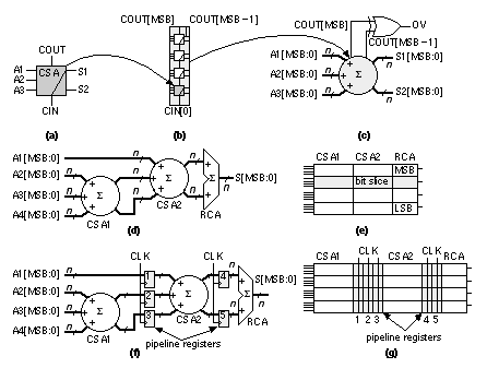
The inputs, A1, A2, and A3; and outputs, S1 and S2, are buses. The input, CIN, is the carry from stage ( i – 1). The carry in, CIN, is connected directly to the output bus S1—indicated by the schematic symbol (Figure 2.23a). We connect CIN[0] to VSS. The output, COUT, is the carry out to stage ( i + 1). A 4-bit CSA is shown in Figure 2.23(b). The arithmetic overflow signal for ones’ complement or two’s complement arithmetic, OV, is XOR(COUT[MSB], COUT[MSB – 1]) as shown in Figure 2.23(c). In a CSA the carries are “saved” at each stage and shifted left onto the bus S1. There is thus no carry propagation and the delay of a CSA is constant. At the output of a CSA we still need to add the S1 bus (all the saved carries) and the S2 bus (all the sums) to get an n -bit result using a final stage that is not shown in Figure 2.23(c). We might regard the n -bit sum as being encoded in the two buses, S1 and S2, in the form of the parity and majority functions. We can use a CSA to add multiple inputs—as an example, an adder with four 4-bit inputs is shown in Figure 2.23(d). The last stage sums two input buses using a carry-propagate adder ( CPA ). We have used an RCA as the CPA in Figure 2.23(d) and (e), but we can use any type of adder. Notice in Figure 2.23(e) how the two CSA cells and the RCA cell abut together horizontally to form a bit slice (or slice) and then the slices are stacked vertically to form the datapath. We can register the CSA stages by adding vectors of flip-flops as shown in Figure 2.23(f). This reduces the adder delay to that of the slowest adder stage, usually the CPA. By using registers between stages of combinational logic we use pipelining to increase the speed and pay a price of increased area (for the registers) and introduce latency . It takes a few clock cycles (the latency, equal to n clock cycles for an n -stage pipeline) to fill the pipeline, but once it is filled, the answers emerge every clock cycle. Ferris wheels work much the same way. When the fair opens it takes a while (latency) to fill the wheel, but once it is full the people can get on and off every few seconds. (We can also pipeline the RCA of Figure 2.20. We add i registers on the A and B inputs before ADD[ i ] and add ( n – i ) registers after the output S[ i ], with a single register before each C[ i ].) The problem with an RCA is that every stage has to wait to make its carry decision, C[ i ], until the previous stage has calculated C[ i – 1]. If we examine the propagate signals we can bypass this critical path. Thus, for example, to bypass the carries for bits 4–7 (stages 5–8) of an adder we can compute BYPASS = P[4].P[5].P[6].P[7] and then use a MUX as follows: Adders based on this principle are called carry-bypass adders ( CBA ) [Sato et al., 1992]. Large, custom adders employ Manchester-carry chains to compute the carries and the bypass operation using TGs or just pass transistors [Weste and Eshraghian, 1993, pp. 530–531]. These types of carry chains may be part of a predesigned ASIC adder cell, but are not used by ASIC designers. Instead of checking the propagate signals we can check the inputs. For example we can compute SKIP = (A[ i – 1] ⊕ B[ i – 1]) + (A[ i ] ⊕ B[ i ] ) and then use a 2:1 MUX to select C[ i ]. Thus,
This is a carry-skip adder [Keutzer, Malik, and Saldanha, 1991; Lehman, 1961]. Carry-bypass and carry-skip adders may include redundant logic (since the carry is computed in two different ways—we just take the first signal to arrive). We must be careful that the redundant logic is not optimized away during logic synthesis. If we evaluate Eq. 2.44 recursively for i = 1, we get the following: This result means that we can “look ahead” by two stages and calculate the carry into the third stage (bit 2), which is C[1], using only the first-stage inputs (to calculate G[0]) and the second-stage inputs. This is a carry-lookahead adder ( CLA ) [MacSorley, 1961]. If we continue expanding Eq. 2.44, we find:
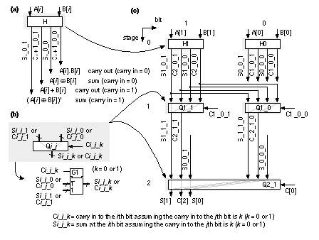
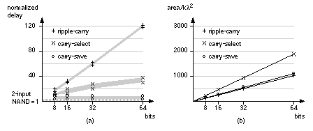
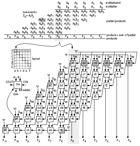
As we look ahead further these equations become more complex, take longer to calculate, and the logic becomes less regular when implemented using cells with a limited number of inputs. Datapath layout must fit in a bit slice, so the physical and logical structure of each bit must be similar. In a standard cell or gate array we are not so concerned about a regular physical structure, but a regular logical structure simplifies design. The Brent–Kung adder reduces the delay and increases the regularity of the carry-lookahead scheme [Brent and Kung, 1982]. Figure 2.24(a) shows a regular 4-bit CLA, using the carry-lookahead generator cell (CLG) shown in Figure 2.24(b). In a carry-select adder we duplicate two small adders (usually 4-bit or 8-bit adders—often CLAs) for the cases CIN = '0' and CIN = '1' and then use a MUX to select the case that we need—wasteful, but fast [Bedrij, 1962]. A carry-select adder is often used as the fast adder in a datapath library because its layout is regular. We can use the carry-select, carry-bypass, and carry-skip architectures to split a 12-bit adder, for example, into three blocks. The delay of the adder is then partly dependent on the delays of the MUX between each block. Suppose the delay due to 1-bit in an adder block (we shall call this a bit delay) is approximately equal to the MUX delay. In this case may be faster to make the blocks 3, 4, and 5-bits long instead of being equal in size. Now the delays into the final MUX are equal—3 bit-delays plus 2 MUX delays for the carry signal from bits 0–6 and 5 bit-delays for the carry from bits 7–11. Adjusting the block size reduces the delay of large adders (more than 16 bits). We can extend the idea behind a carry-select adder as follows. Suppose we have an n -bit adder that generates two sums: One sum assumes a carry-in condition of '0', the other sum assumes a carry-in condition of '1'. We can split this n -bit adder into an i -bit adder for the i LSBs and an ( n – i )-bit adder for the n – i MSBs. Both of the smaller adders generate two conditional sums as well as true and complement carry signals. The two (true and complement) carry signals from the LSB adder are used to select between the two ( n – i + 1)-bit conditional sums from the MSB adder using 2( n – i + 1) two-input MUXes. This is a conditional-sum adder (also often abbreviated to CSA) [Sklansky, 1960]. We can recursively apply this technique. For example, we can split a 16-bit adder using i = 8 and n = 8; then we can split one or both 8–bit adders again—and so on. Figure 2.25 shows the simplest form of an n -bit conditional-sum adder that uses n single-bit conditional adders, H (each with four outputs: two conditional sums, true carry, and complement carry), together with a tree of 2:1 MUXes (Qi_j). The conditional-sum adder is usually the fastest of all the adders we have discussed (it is the fastest when logic cell delay increases with the number of inputs—this is true for all ASICs except FPGAs). 2.6.3 A Simple ExampleHow do we make and use datapath elements? What does a design look like? We may use predesigned cells from a library or build the elements ourselves from logic cells using a schematic or a design language. Table 2.12 shows an 8-bit conditional-sum adder intended for an FPGA. This Verilog implementation uses the same structure as Figure 2.25, but the equations are collapsed to use four or five variables. A basic logic cell in certain Xilinx FPGAs, for example, can implement two equations of the same four variables or one equation with five variables. The equations shown in Table 2.12 requires three levels of FPGA logic cells (so, for example, if each FPGA logic cell has a 5 ns delay, the 8-bit conditional-sum adder delay is 15 ns). Figure 2.26 shows the normalized delay and area figures for a set of predesigned datapath adders. The data in Figure 2.26 is from a series of ASIC datapath cell libraries (Compass Passport) that may be synthesized together with test vectors and simulation models. We can combine the different adder techniques, but the adders then lose regularity and become less suited to a datapath implementation. There are other adders that are not used in datapaths, but are occasionally useful in ASIC design. A serial adder is smaller but slower than the parallel adders we have described [Denyer and Renshaw, 1985]. The carry-completion adder is a variable delay adder and rarely used in synchronous designs [Sklansky, 1960]. 2.6.4 MultipliersFigure 2.27 shows a symmetric 6-bit array multiplier (an n -bit multiplier multiplies two n -bit numbers; we shall use n -bit by m -bit multiplier if the lengths are different). Adders a0–f0 may be eliminated, which then eliminates adders a1–a6, leaving an asymmetric CSA array of 30 (5 ¥ 6) adders (including one half adder). An n -bit array multiplier has a delay proportional to n plus the delay of the CPA (adders b6–f6 in Figure 2.27). There are two items we can attack to improve the performance of a multiplier: the number of partial products and the addition of the partial products. Suppose we wish to multiply 15 (the multiplicand ) by 19 (the multiplier ) mentally. It is easier to calculate 15 ¥ 20 and subtract 15. In effect we complete the multiplication as 15 ¥ (20 – 1) and we could write this as 15 ¥ 2 1 , with the overbar representing a minus sign. Now suppose we wish to multiply an 8-bit binary number, A, by B = 00010111 (decimal 16 + 4 + 2 + 1 = 23). It is easier to multiply A by the canonical signed-digit vector ( CSD vector ) D = 0010 1 001 (decimal 32 – 8 + 1 = 23) since this requires only three add or subtract operations (and a subtraction is as easy as an addition). We say B has a weight of 4 and D has a weight of 3. By using D instead of B we have reduced the number of partial products by 1 (= 4 – 3). We can recode (or encode) any binary number, B, as a CSD vector, D, as follows (canonical means there is only one CSD vector for any number): where C i + 1 is the carry from the sum of B i + 1 + B i + C i (we start with C 0 = 0). As another example, if B = 011 (B 2 = 0, B 1 = 1, B 0 = 1; decimal 3), then, using Eq. 2.58, so that D = 10 1 (decimal 4 – 1 = 3). CSD vectors are useful to represent fixed coefficients in digital filters, for example. We can recode using a radix other than 2. Suppose B is an ( n + 1)-digit two’s complement number,
We can rewrite the expression for B using the following sleight-of-hand:
This is very useful. Consider B = 101001 (decimal 9 – 32 = –23, n = 5),
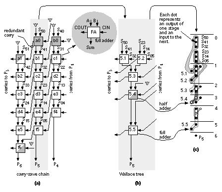
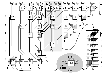
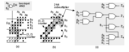
Equation 2.61 tells us how to encode B as a radix-4 signed digit, E = 12 1 (decimal –16 – 8 + 1 = –23). To multiply by B encoded as E we only have to perform a multiplication by 2 (a shift) and three add/subtract operations. Using Eq. 2.61 we can encode any number by taking groups of three bits at a time and calculating where each 3-bit group overlaps by one bit. We pad B with a zero, B n . . . B 1 B 0 0, to match the first term in Eq. 2.61. If B has an odd number of bits, then we extend the sign: B n B n . . . B 1 B 0 0. For example, B = 01011 (eleven), encodes to E = 1 11 (16 – 4 – 1); and B = 101 is E = 1 1. This is called Booth encoding and reduces the number of partial products by a factor of two and thus considerably reduces the area as well as increasing the speed of our multiplier [Booth, 1951]. Next we turn our attention to improving the speed of addition in the CSA array. Figure 2.28(a) shows a section of the 6-bit array multiplier from Figure 2.27. We can collapse the chain of adders a0–f5 (5 adder delays) to the Wallace tree consisting of adders 5.1–5.4 (4 adder delays) shown in Figure 2.28(b). Figure 2.28(c) pictorially represents multiplication as a sort of golf course. Each link corresponds to an adder. The holes or dots are the outputs of one stage (and the inputs of the next). At each stage we have the following three choices: (1) sum three outputs using a full adder (denoted by a box enclosing three dots); (2) sum two outputs using a half adder (a box with two dots); (3) pass the outputs directly to the next stage. The two outputs of an adder are joined by a diagonal line (full adders use black dots, half adders white dots). The object of the game is to choose (1), (2), or (3) at each stage to maximize the performance of the multiplier. In tree-based multipliers there are two ways to do this—working forward and working backward. In a Wallace-tree multiplier we work forward from the multiplier inputs, compressing the number of signals to be added at each stage [Wallace, 1960]. We can view an FA as a 3:2 compressor or (3, 2) counter —it counts the number of '1's on the inputs. Thus, for example, an input of '101' (two '1's) results in an output '10' (2). A half adder is a (2, 2) counter . To form P 5 in Figure 2.29 we must add 6 summands (S 05 , S 14 , S 23 , S 32 , S 41 , and S 50 ) and 4 carries from the P 4 column. We add these in stages 1–7, compressing from 6:3:2:2:3:1:1. Notice that we wait until stage 5 to add the last carry from column P 4 , and this means we expand (rather than compress) the number of signals (from 2 to 3) between stages 3 and 5. The maximum delay through the CSA array of Figure 2.29 is 6 adder delays. To this we must add the delay of the 4-bit (9 inputs) CPA (stage 7). There are 26 adders (6 half adders) plus the 4 adders in the CPA. In a Dadda multiplier (Figure 2.30) we work backward from the final product [Dadda, 1965]. Each stage has a maximum of 2, 3, 4, 6, 9, 13, 19, . . . outputs (each successive stage is 3/2 times larger—rounded down to an integer). Thus, for example, in Figure 2.28(d) we require 3 stages (with 3 adder delays—plus the delay of a 10-bit output CPA) for a 6-bit Dadda multiplier. There are 19 adders (4 half adders) in the CSA plus the 10 adders (2 half adders) in the CPA. A Dadda multiplier is usually faster and smaller than a Wallace-tree multiplier. In general, the number of stages and thus delay (in units of an FA delay—excluding the CPA) for an n -bit tree-based multiplier using (3, 2) counters is Figure 2.31(a) shows how the partial-product array is constructed in a conventional 4-bit multiplier. The Ferrari–Stefanelli multiplier (Figure 2.31b) “nests” multipliers—the 2-bit submultipliers reduce the number of partial products [Ferrari and Stefanelli, 1969]. There are several issues in deciding between parallel multiplier architectures:
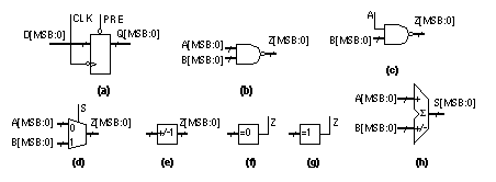
2.6.5 Other Arithmetic SystemsThere are other schemes for addition and multiplication that are useful in special circumstances. Addition of numbers using redundant binary encoding avoids carry propagation and is thus potentially very fast. Table 2.13 shows the rules for addition using an intermediate carry and sum that are added without the need for carry. For example, The redundant binary representation is not unique. We can represent 101 (decimal), for example, by 1100101 (binary and CSD vector) or 1 1 100111. As another example, 188 (decimal) can be represented by 10111100 (binary), 1 1 1000 1 00, 10 1 00 1 100, or 10 1 000 1 00 (CSD vector). Redundant binary addition of binary, redundant binary, or CSD vectors does not result in a unique sum, and addition of two CSD vectors does not result in a CSD vector. Each n -bit redundant binary number requires a rather wasteful 2 n -bit binary number for storage. Thus 10 1 is represented as 010010, for example (using sign magnitude). The other disadvantage of redundant binary arithmetic is the need to convert to and from binary representation. Table 2.14 shows the (5, 3) residue number system . As an example, 11 (decimal) is represented as [1, 2] residue (5, 3) since 11R 5 = 11 mod 5 = 1 and 11R 3 = 11 mod 3 = 2. The size of this system is thus 3 ¥ 5 = 15. We add, subtract, or multiply residue numbers using the modulus of each bit position—without any carry. Thus: The choice of moduli determines the system size and the computing complexity. The most useful choices are relative primes (such as 3 and 5). With p prime, numbers of the form 2 p and 2 p – 1 are particularly useful (2 p – 1 are Mersenne’s numbers ) [Waser and Flynn, 1982]. 2.6.6 Other Datapath OperatorsFigure 2.32 shows symbols for some other datapath elements. The combinational datapath cells, NAND, NOR, and so on, and sequential datapath cells (flip-flops and latches) have standard-cell equivalents and function identically. I use a bold outline (1 point) for datapath cells instead of the regular (0.5 point) line I use for scalar symbols. We call a set of identical cells a vector of datapath elements in the same way that a bold symbol, A , represents a vector and A represents a scalar. A subtracter is similar to an adder, except in a full subtracter we have a borrow-in signal, BIN; a borrow-out signal, BOUT; and a difference signal, DIFF: These equations are the same as those for the FA (Eqs. 2.38 and 2.39) except that the B input is inverted and the sense of the carry chain is inverted. To build a subtracter that calculates (A – B) we invert the entire B input bus and connect the BIN[0] input to VDD (not to VSS as we did for CIN[0] in an adder). As an example, to subtract B = '0011' from A = '1001' we calculate '1001' + '1100' + '1' = '0110'. As with an adder, the true overflow is XOR(BOUT[MSB], BOUT[MSB – 1]). We can build a ripple-borrow subtracter (a type of borrow-propagate subtracter), a borrow-save subtracter, and a borrow-select subtracter in the same way we built these adder architectures. An adder/subtracter has a control signal that gates the A input with an exclusive-OR cell (forming a programmable inversion) to switch between an adder or subtracter. Some adder/subtracters gate both inputs to allow us to compute (–A – B). We must be careful to connect the input to the LSB of the carry chain (CIN[0] or BIN[0]) when changing between addition (connect to VSS) and subtraction (connect to VDD). A barrel shifter rotates or shifts an input bus by a specified amount. For example if we have an eight-input barrel shifter with input '1111 0000' and we specify a shift of '0001 0000' (3, coded by bit position) the right-shifted 8-bit output is '0001 1110'. A barrel shifter may rotate left or right (or switch between the two under a separate control). A barrel shifter may also have an output width that is smaller than the input. To use a simple example, we may have an 8-bit input and a 4-bit output. This situation is equivalent to having a barrel shifter with two 4-bit inputs and a 4-bit output. Barrel shifters are used extensively in floating-point arithmetic to align (we call this normalize and denormalize ) floating-point numbers (with sign, exponent, and mantissa). A leading-one detector is used with a normalizing (left-shift) barrel shifter to align mantissas in floating-point numbers. The input is an n -bit bus A, the output is an n -bit bus, S, with a single '1' in the bit position corresponding to the most significant '1' in the input. Thus, for example, if the input is A = '0000 0101' the leading-one detector output is S = '0000 0100', indicating the leading one in A is in bit position 2 (bit 7 is the MSB, bit zero is the LSB). If we feed the output, S, of the leading-one detector to the shift select input of a normalizing (left-shift) barrel shifter, the shifter will normalize the input A. In our example, with an input of A = '0000 0101', and a left-shift of S = '0000 0100', the barrel shifter will shift A left by five bits and the output of the shifter is Z = '1010 0000'. Now that Z is aligned (with the MSB equal to '1') we can multiply Z with another normalized number. The output of a priority encoder is the binary-encoded position of the leading one in an input. For example, with an input A = '0000 0101' the leading 1 is in bit position 3 (MSB is bit position 7) so the output of a 4-bit priority encoder would be Z = '0011' (3). In some cell libraries the encoding is reversed so that the MSB has an output code of zero, in this case Z = '0101' (5). This second, reversed, encoding scheme is useful in floating-point arithmetic. If A is a mantissa and we normalize A to '1010 0000' we have to subtract 5 from the exponent, this exponent correction is equal to the output of the priority encoder. An accumulator is an adder/subtracter and a register. Sometimes these are combined with a multiplier to form a multiplier–accumulator ( MAC ). An incrementer adds 1 to the input bus, Z = A + 1, so we can use this function, together with a register, to negate a two’s complement number for example. The implementation is Z[ i ] = XOR(A[ i ], CIN[ i ]), and COUT[ i ] = AND(A[ i ], CIN[ i ]). The carry-in control input, CIN[0], thus acts as an enable: If it is set to '0' the output is the same as the input. The implementation of arithmetic cells is often a little more complicated than we have explained. CMOS logic is naturally inverting, so that it is faster to implement an incrementer as Z[ i (even)] = XOR(A[ i ], CIN[ i ]) and COUT[ i (even)] = NAND(A[ i ], CIN[ i ]). This inverts COUT, so that in the following stage we must invert it again. If we push an inverting bubble to the input CIN we find that: Z[ i (odd)] = XNOR(A[ i ], CIN[ i ]) and COUT[ i (even)] = NOR(NOT(A[ i ]), CIN[ i ]). In many datapath implementations all odd-bit cells operate on inverted carry signals, and thus the odd-bit and even-bit datapath elements are different. In fact, all the adder and subtracter datapath elements we have described may use this technique. Normally this is completely hidden from the designer in the datapath assembly and any output control signals are inverted, if necessary, by inserting buffers. A decrementer subtracts 1 from the input bus, the logical implementation is Z[ i ] = XOR(A[ i ], CIN[ i ]) and COUT[ i ] = AND(NOT(A[ i ]), CIN[ i ]). The implementation may invert the odd carry signals, with CIN[0] again acting as an enable. An incrementer/decrementer has a second control input that gates the input, inverting the input to the carry chain. This has the effect of selecting either the increment or decrement function. Using the all-zeros detectors and all-ones detectors , remember that, for a 4-bit number, for example, zero in ones’ complement arithmetic is '1111' or '0000', and that zero in signed magnitude arithmetic is '1000' or '0000'. A register file (or scratchpad memory) is a bank of flip-flops arranged across the bus; sometimes these have the option of multiple ports (multiport register files) for read and write. Normally these register files are the densest logic and hardest to fit in a datapath. For large register files it may be more appropriate to use a multiport memory. We can add control logic to a register file to create a first-in first-out register ( FIFO ), or last-in first-out register ( LIFO ). In Section 2.5 we saw that the standard-cell version and gate-array macro version of the sequential cells (latches and flip-flops) each contain their own clock buffers. The reason for this is that (without intelligent placement software) we do not know where a standard cell or a gate-array macro will be placed on a chip. We also have no idea of the condition of the clock signal coming into a sequential cell. The ability to place the clock buffers outside the sequential cells in a datapath gives us more flexibility and saves space. For example, we can place the clock buffers for all the clocked elements at the top of the datapath (together with the buffers for the control signals) and river route (in river routing the interconnect lines all flow in the same direction on the same layer) the connections to the clock lines. This saves space and allows us to guarantee the clock skew and timing. It may mean, however, that there is a fixed overhead associated with a datapath. For example, it might make no sense to build a 4-bit datapath if the clock and control buffers take up twice the space of the datapath logic. Some tools allow us to design logic using a portable netlist . After we complete the design we can decide whether to implement the portable netlist in a datapath, standard cells, or even a gate array, based on area, speed, or power considerations. [ Chapter start ] [ Previous page ] [ Next page ] | ||||||||||||||||||||||||||||||||||||||||||||||||||||||||||||||||||||||||||||||||||||||||||||||||||||||||||||||||||||||||||||||||||||||||||||||||||||||||||||||||||||||||||||||||||||||||||||||||||||||||||||||||||||||||||||||||||||||||||||||||||||||||||||||||||||||||||||||||||||||||||||||||||||||||||||||||||||||||||||||||||||||||||||||||||||||||||||||||||||||||||||||||||||||||||||||||||||||||||||||||
