|
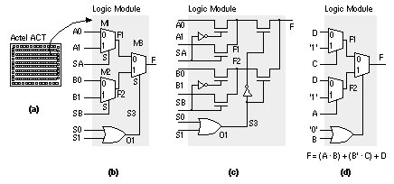
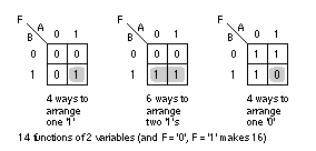
[ Chapter start ] [ Previous page ] [ Next page ] 5.1 Actel ACTThe basic logic cells in the Actel ACT family of FPGAs are called Logic Modules . The ACT 1 family uses just one type of Logic Module and the ACT 2 and ACT 3 FPGA families both use two different types of Logic Module. 5.1.1 ACT 1 Logic ModuleThe functional behavior of the Actel ACT 1 Logic Module is shown in Figure 5.1 (a). Figure 5.1 (b) represents a possible circuit-level implementation. We can build a logic function using an Actel Logic Module by connecting logic signals to some or all of the Logic Module inputs, and by connecting any remaining Logic Module inputs to VDD or GND. As an example, Figure 5.1 (c) shows the connections to implement the function F = A · B + B' · C + D. How did we know what connections to make? To understand how the Actel Logic Module works, we take a detour via multiplexer logic and some theory. 5.1.2 Shannon’s Expansion TheoremIn logic design we often have to deal with functions of many variables. We need a method to break down these large functions into smaller pieces. Using the Shannon expansion theorem, we can expand a Boolean logic function F in terms of (or with respect to) a Boolean variable A, F = A · F (A = '1') + A' · F (A = '0'),(5.1) where F (A = 1) represents the function F evaluated with A set equal to '1'. For example, we can expand the following function F with respect to (I shall use the abbreviation wrt ) A, F = A' · B + A · B · C' + A' · B' · C = A · (B · C') + A' · (B + B' · C).(5.2) We have split F into two smaller functions. We call F (A = '1') = B · C' the cofactor of F wrt A in Eq. 5.2 . I shall sometimes write the cofactor of F wrt A as F A (the cofactor of F wrt A' is F A' ). We may expand a function wrt any of its variables. For example, if we expand F wrt B instead of A, F = A' · B + A · B · C' + A' · B' · C = B · (A' + A · C') + B' · (A' · C).(5.3) We can continue to expand a function as many times as it has variables until we reach the canonical form (a unique representation for any Boolean function that uses only minterms. A minterm is a product term that contains all the variables of F—such as A · B' · C). Expanding Eq. 5.3 again, this time wrt C, gives F = C · (A' · B + A' · B') + C' · (A · B + A' · B).(5.4) As another example, we will use the Shannon expansion theorem to implement the following function using the ACT 1 Logic Module: F = (A · B) + (B' · C) + D.(5.5) F = B · (A + D) + B' · (C + D) Equation 5.6 describes a 2:1 MUX, with B selecting between two inputs: F (A = '1') and F (A = '0'). In fact Eq. 5.6 also describes the output of the ACT 1 Logic Module in Figure 5.1 ! Now we need to split up F1 and F2 in Eq. 5.6 . Suppose we expand F2 = F B wrt A, and F1 = F B' wrt C: F2 = A + D = (A · 1) + (A' · D),(5.7) F1 = C + D = (C · 1) + (C' · D).(5.8) From Eqs. 5.6 – 5.8 we see that we may implement F by arranging for A, B, C to appear on the select lines and '1' and D to be the data inputs of the MUXes in the ACT 1 Logic Module. This is the implementation shown in Figure 5.1 (d), with connections: A0 = D, A1 = '1', B0 = D, B1 = '1', SA = C, SB = A, S0 = '0', and S1 = B. Now that we know that we can implement Boolean functions using MUXes, how do we know which functions we can implement and how to implement them? 5.1.3 Multiplexer Logic as Function GeneratorsFigure 5.2 illustrates the 16 different ways to arrange ‘1’s on a Karnaugh map corresponding to the 16 logic functions, F (A, B), of two variables. Two of these functions are not very interesting (F = '0', and F = '1'). Of the 16 functions, Table 5.1 shows the 10 that we can implement using just one 2:1 MUX. Of these 10 functions, the following six are useful:
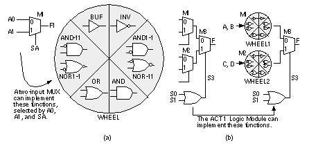
Figure 5.3 (a) shows how we might view a 2:1 MUX as a function wheel , a three-input black box that can generate any one of the six functions of two-input variables: BUF, INV, AND-11, AND1-1, OR, AND. We can write the output of a function wheel as where I define the wheel function as follows: WHEEL1 (A, B) = MUX (A0, A1, SA).(5.10) The MUX function is not unique; we shall define it as MUX (A0, A1, SA) = A0 · SA' + A1 · SA.(5.11) The inputs (A0, A1, SA) are described using the notation A0, A1, SA = {A, B, '0', '1'}(5.12) to mean that each of the inputs (A0, A1, and SA) may be any of the values: A, B, '0', or '1'. I chose the name of the wheel function because it is rather like a dial that you set to your choice of function. Figure 5.3 (b) shows that the ACT 1 Logic Module is a function generator built from two function wheels, a 2:1 MUX, and a two-input OR gate.
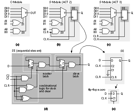
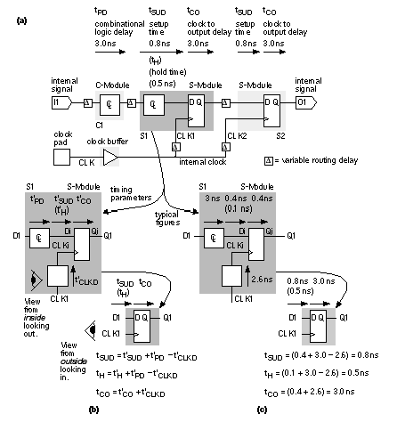
We can describe the ACT 1 Logic Module in terms of two WHEEL functions: F = MUX [ WHEEL1, WHEEL2, OR (S0, S1) ](5.13) Now, for example, to implement a two-input NAND gate, F = NAND (A, B) = (A · B)', using an ACT 1 Logic Module we first express F as the output of a 2:1 MUX. To split up F we expand it wrt A (or wrt B; since F is symmetric in A and B): F = A · (B') + A' · ('1')(5.14) Thus to make a two-input NAND gate we assign WHEEL1 to implement INV (B), and WHEEL2 to implement '1'. We must also set the select input to the MUX connecting WHEEL1 and WHEEL2, S0 + S1 = A—we can do this with S0 = A, S1 = '1'. Before we get too carried away, we need to realize that we do not have to worry about how to use Logic Modules to construct combinational logic functions—this has already been done for us. For example, if we need a two-input NAND gate, we just use a NAND gate symbol and software takes care of connecting the inputs in the right way to the Logic Module. How did Actel design its Logic Modules? One of Actel’s engineers wrote a program that calculates how many functions of two, three, and four variables a given circuit would provide. The engineers tested many different circuits and chose the best one: a small, logically efficient circuit that implemented many functions. For example, the ACT 1 Logic Module can implement all two-input functions, most functions with three inputs, and many with four inputs. Apart from being able to implement a wide variety of combinational logic functions, the ACT 1 module can implement sequential logic cells in a flexible and efficient manner. For example, you can use one ACT 1 Logic Module for a transparent latch or two Logic Modules for a flip-flop. The use of latches rather than flip-flops does require a shift to a two-phase clocking scheme using two nonoverlapping clocks and two clock trees. Two-phase synchronous design using latches is efficient and fast but, to handle the timing complexities of two clocks requires changes to synthesis and simulation software that have not occurred. This means that most people still use flip-flops in their designs, and these require two Logic Modules. 5.1.4 ACT 2 and ACT 3 Logic ModulesUsing two ACT 1 Logic Modules for a flip-flop also requires added interconnect and associated parasitic capacitance to connect the two Logic Modules. To produce an efficient two-module flip-flop macro we could use extra antifuses in the Logic Module to cut down on the parasitic connections. However, the extra antifuses would have an adverse impact on the performance of the Logic Module in other macros. The alternative is to use a separate flip-flop module, reducing flexibility and increasing layout complexity. In the ACT 1 family Actel chose to use just one type of Logic Module. The ACT 2 and ACT 3 architectures use two different types of Logic Modules, and one of them does include the equivalent of a D flip-flop. Figure 5.4 shows the ACT 2 and ACT 3 Logic Modules. The ACT 2 C-Module is similar to the ACT 1 Logic Module but is capable of implementing five-input logic functions. Actel calls its C-module a combinatorial module even though the module implements combinational logic. John Wakerly blames MMI for the introduction of the term combinatorial [Wakerly, 1994, p. 404]. The use of MUXes in the Actel Logic Modules (and in other places) can cause confusion in using and creating logic macros. For the Actel library, setting S = '0' selects input A of a two-input MUX. For other libraries setting S = '1' selects input A. This can lead to some very hard to find errors when moving schematics between libraries. Similar problems arise in flip-flops and latches with MUX inputs. A safer way to label the inputs of a two-input MUX is with '0' and '1', corresponding to the input selected when the select input is '1' or '0'. This notation can be extended to bigger MUXes, but in Figure 5.4 , does the input combination S0 = '1' and S1 = '0' select input D10 or input D01? These problems are not caused by Actel, but by failure to use the IEEE standard symbols in this area. The S-Module ( sequential module ) contains the same combinational function capability as the C-Module together with a sequential element that can be configured as a flip-flop. Figure 5.4 (d) shows the sequential element implementation in the ACT 2 and ACT 3 architectures. 5.1.5 Timing Model and Critical PathFigure 5.5 (a) shows the timing model for the ACT family. 5 This is a simple timing model since it deals only with logic buried inside a chip and allows us only to estimate delays. We cannot predict the exact delays on an Actel chip until we have performed the place-and-route step and know how much delay is contributed by the interconnect. Since we cannot determine the exact delay before physical layout is complete, we call the Actel architecture nondeterministic . Even though we cannot determine the preroute delays exactly, it is still important to estimate the delay on a logic path. For example, Figure 5.5 (a) shows a typical situation deep inside an ASIC. Internal signal I1 may be from the output of a register (flip-flop). We then pass through some combinational logic, C1, through a register, S1, and then another register, S2. The register-to-register delay consists of a clock–Q delay, plus any combinational delay between registers, and the setup time for the next flip-flop. The speed of our system will depend on the slowest register–register delay or critical path between registers. We cannot make our clock period any longer than this or the signal will not reach the second register in time to be clocked. Figure 5.5 (a) shows an internal logic signal, I1, that is an input to a C-module, C1. C1 is drawn in Figure 5.5 (a) as a box with a symbol comprising the overlapping letters “C” and “L” (borrowed from carpenters who use this symbol to mark the centerline on a piece of wood). We use this symbol to describe combinational logic. For the standard-speed grade ACT 3 (we shall look at speed grading in Section 5.1.6 ) the delay between the input of a C-module and the output is specified in the data book as a parameter, t PD , with a maximum value of 3.0 ns. The output of C1 is an input to an S-Module, S1, configured to implement combinational logic and a D flip-flop. The Actel data book specifies the minimum setup time for this D flip-flop as t SUD = 0.8 ns. This means we need to get the data to the input of S1 at least 0.8 ns before the rising clock edge (for a positive-edge–triggered flip-flop). If we do this, then there is still enough time for the data to go through the combinational logic inside S1 and reach the input of the flip-flop inside S1 in time to be clocked. We can guarantee that this will work because the combinational logic delay inside S1 is fixed.
The S-Module seems like good value—we get all the combinational logic functions of a C-module (with delay t PD of 3 ns) as well as the setup time for a flip-flop for only 0.8 ns? …not really. Next I will explain why not. Figure 5.5 (b) shows what is happening inside an S-Module. The setup and hold times, as measured inside (not outside) the S-Module, of the flip-flop are t' SUD and t' H (a prime denotes parameters that are measured inside the S-Module). The clock–Q propagation delay is t' CO . The parameters t' SUD , t' H , and t' CO are measured using the internal clock signal CLKi. The propagation delay of the combinational logic inside the S-Module is t' PD . The delay of the combinational logic that drives the flip-flop clock signal ( Figure 5.4 d) is t' CLKD . From outside the S-Module, with reference to the outside clock signal CLK1: t SUD = t' SUD + (t' PD – t' CLKD ), t H = t' H + (t' PD – t' CLKD ), t CO = t' CO + t' CLKD .(5.15) Figure 5.5 (c) shows an example of flip-flop timing. We have no way of knowing what the internal flip-flop parameters t' SUD , t' H , and t' CO actually are, but we can assume some reasonable values (just for illustration purposes): t' SUD = 0.4 ns, t' H = 0.1 ns, t' CO = 0.4 ns.(5.16) We do know the delay, t' PD , of the combinational logic inside the S-Module. It is exactly the same as the C-Module delay, so t' PD = 3 ns for the ACT 3. We do not know t' CLKD ; we shall assume a reasonable value of t' CLKD = 2.6 ns (the exact value does not matter in the following argument). Next we calculate the external S-Module parameters from Eq. 5.15 as follows: t SUD = 0.8 ns, t H = 0.5 ns, t CO = 3.0 ns.(5.17) These are the same as the ACT 3 S-Module parameters shown in Figure 5.5 (a), and I chose t' CLKD and the values in Eq. 5.16 so that they would be the same. So now we see where the combinational logic delay of 3.0 ns has gone: 0.4 ns went into increasing the setup time and 2.6 ns went into increasing the clock–output delay, t CO . From the outside we can say that the combinational logic delay is buried in the flip-flop setup time. FPGA vendors will point this out as an advantage that they have. Of course, we are not getting something for nothing here. It is like borrowing money—you have to pay it back. 5.1.6 Speed GradingMost FPGA vendors sort chips according to their speed ( the sorting is known as speed grading or speed binning , because parts are automatically sorted into plastic bins by the production tester). You pay more for the faster parts. In the case of the ACT family of FPGAs, Actel measures performance with a special binning circuit , included on every chip, that consists of an input buffer driving a string of buffers or inverters followed by an output buffer. The parts are sorted from measurements on the binning circuit according to Logic Module propagation delay. The propagation delay, t PD , is defined as the average of the rising ( t PLH ) and falling ( t PHL ) propagation delays of a Logic Module t PD = ( t PLH + t PHL )/2.(5.18) Since the transistor properties match so well across a chip, measurements on the binning circuit closely correlate with the speed of the rest of the Logic Modules on the die. Since the speeds of die on the same wafer also match well, most of the good die on a wafer fall into the same speed bin. Actel speed grades are: a 'Std' speed grade, a '1' speed grade that is approximately 15 percent faster, a '2' speed grade that is approximately 25 percent faster than 'Std', and a '3' speed grade that is approximately 35 percent faster than 'Std'. 5.1.7 Worst-Case TimingIf you use fully synchronous design techniques you only have to worry about how slow your circuit may be—not how fast. Designers thus need to know the maximum delays they may encounter, which we call the worst-case timing . Maximum delays in CMOS logic occur when operating under minimum voltage, maximum temperature, and slow–slow process conditions. (A slow–slow process refers to a process variation, or process corner , which results in slow p -channel transistors and slow n -channel transistors—we can also have fast–fast, slow–fast, and fast–slow process corners.) Electronic equipment has to survive in a variety of environments and ASIC manufacturers offer several classes of qualification for different applications:
ASICs for commercial application are cheapest; ASICs for the Cruise missile are very, very expensive. Notice that commercial and industrial application parts are specified with respect to the ambient temperature T A (room temperature or the temperature inside the box containing the ASIC). Military specifications are relative to the package case temperature , T C . What is really important is the temperature of the transistors on the chip, the junction temperature , T J , which is always higher than T A (unless we dissipate zero power). For most applications that dissipate a few hundred mW, T J is only 5–10 °C higher than T A . To calculate the value of T J we need to know the power dissipated by the chip and the thermal properties of the package—we shall return to this in Section 6.6.1, “Power Dissipation.” Manufacturers have to specify their operating conditions with respect to T J and not T A , since they have no idea how much power purchasers will dissipate in their designs or which package they will use. Actel used to specify timing under nominal operating conditions: VDD = 5.0 V, and T J = 25 °C. Actel and most other manufacturers now specify parameters under worst-case commercial conditions: VDD = 4.75 V, and T J = +70 °C. Table 5.2 shows the ACT 3 commercial worst-case timing. 6 In this table Actel has included some estimates of the variable routing delay shown in Figure 5.5 (a). These delay estimates depend on the number of gates connected to a gate output (the fanout). When you design microelectronic systems (or design anything ) you must use worst-case figures ( just as you would design a bridge for the worst-case load). To convert nominal or typical timing figures to the worst case (or best case), we use measured, or empirically derived, constants called derating factors that are expressed either as a table or a graph. For example, Table 5.3 shows the ACT 3 derating factors from commercial worst-case to industrial worst-case and military worst-case conditions (assuming T J = T A ). The ACT 1 and ACT 2 derating factors are approximately the same. 7
As an example of a timing calculation, suppose we have a Logic Module on a 'Std' speed grade A1415A (an ACT 3 part) that drives four other Logic Modules and we wish to estimate the delay under worst-case industrial conditions. From the data in Table 5.2 we see that the Logic Module delay for an ACT 3 'Std' part with a fanout of four is t PD = 5.7 ns (commercial worst-case conditions, assuming T J = T A ). If this were the slowest path between flip-flops (very unlikely since we have only one stage of combinational logic in this path), our estimated critical path delay between registers , t CRIT , would be the combinational logic delay plus the flip-flop setup time plus the clock–output delay: t CRIT (w-c commercial) = t PD + t SUD + t CO = 5.7 ns + 0.8 ns + 3.0 ns = 9.5 ns .(5.19) (I use w-c as an abbreviation for worst-case.) Next we need to adjust the timing to worst-case industrial conditions. The appropriate derating factor is 1.07 (from Table 5.3 ); so the estimated delay is t CRIT (w-c industrial) = 1.07 ¥ 9.5 ns = 10.2 ns .(5.20) Let us jump ahead a little and assume that we can calculate that T J = T A + 20 °C = 105 °C in our application. To find the derating factor at 105 °C we linearly interpolate between the values for 85 °C (1.07) and 125 °C (1.17) from Table 5.3 ). The interpolated derating factor is 1.12 and thus t CRIT (w-c industrial, T J = 105 °C) = 1.12 ¥ 9.5 ns = 10.6 ns ,(5.21) giving us an operating frequency of just less than 100 MHz. It may seem unfair to calculate the worst-case performance for the slowest speed grade under the harshest industrial conditions—but the examples in the data books are always for the fastest speed grades under less stringent commercial conditions. If we want to illustrate the use of derating, then the delays can only get worse than the data book values! The ultimate word on logic delays for all FPGAs is the timing analysis provided by the FPGA design tools. However, you should be able to calculate whether or not the answer that you get from such a tool is reasonable. 5.1.8 Actel Logic Module AnalysisThe sizes of the ACT family Logic Modules are close to the size of the base cell of an MGA. We say that the Actel ACT FPGAs use a fine-grain architecture . An advantage of a fine-grain architecture is that, whatever the mix of combinational logic to flip-flops in your application, you can probably still use 90 percent of an Actel FPGA. Another advantage is that synthesis software has an easier time mapping logic efficiently to the simple Actel modules. The physical symmetry of the ACT Logic Modules greatly simplifies the place-and-route step. In many cases the router can swap equivalent pins on opposite sides of the module to ease channel routing. The design of the Actel Logic Modules is a balance between efficiency of implementation and efficiency of utilization. A simple Logic Module may reduce performance in some areas—as I have pointed out—but allows the use of fast and robust place-and-route software. Fast, robust routing is an important part of Actel FPGAs (see Section 7.1, “Actel ACT”). 1. The minterm numbers are formed from the product terms of the canonical form. For example, A · B' = 10 = 2. 4. Connections to a two-input MUX: A0 and A1 are the data inputs and SA is the select input (see Eq. 5.11 ). 8. V DD = 4.75 V, T J ( junction) = 70 °C. Logic module plus routing delay. All propagation delays in nanoseconds. [ Chapter start ] [ Previous page ] [ Next page ] | |||||||||||||||||||||||||||||||||||||||||||||||||||||||||||||||||||||||||||||||||||||||||||||||||||||||||||||||||||||||||||||||||||||||||||||||||||||||||||||||||||||||||||||||||||||||||||||||||||||||||||||||||||||||||||||||||||||||||||||||||||||||||||||||||

