12.1  A Logic-Synthesis Example

As an example of logic synthesis, we will compare two implementations of the Viterbi decoder described in Chapter 11. Both versions used logic cells from a VLSI Technology cell library. The first ASIC was designed by hand using schematic entry and a data book. The second version of the ASIC (the one that was fabricated) used Verilog for design entry and a logic synthesizer. Table 12.1 compares the two versions. The synthesized ASIC is 16 percent smaller and 13 percent faster than the hand-designed version.

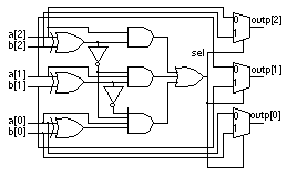
How does logic synthesis generate smaller and faster circuits? Figure 12.1 shows the schematic for a hand-designed comparator and MUX used in the Viterbi decoder ASIC, called here the comparator/MUX example. The Verilog code and the schematic in Figure 12.1 describe the same function. The comparison, in Table 12.2 , of the two design approaches shows that the synthesized version is smaller and faster than the hand design, even though the synthesized design uses more cells.

TABLE 12.1  A comparison of hand design with synthesis (using a 1.0 m m VLSI Technology cell library).


Path delay/
ns
( 1 )

No. of standard cells

No. of transistors

Chip area/
mils
2 ( 2 )

Hand design

41.6

1,359

16,545

21,877

Synthesized design

36.3

1,493

11,946

18,322


// comp_mux.v

module comp_mux(a, b, outp);

input [2:0] a, b;

output [2:0] outp;

function [2:0] compare;

input [2:0] ina, inb;

begin

if (ina <= inb) compare = ina;

else compare = inb;

end

endfunction

assign outp = compare(a, b);

endmodule

FIGURE 12.1  Schematic and HDL design entry.

TABLE 12.2  Comparison of the comparator/MUX designs using a 1.0 m m standard-cell library.


Delay /ns

No. of standard cells

No. of transistors

Area /mils 2

Hand design

4.3

12

116

68.68

Synthesized

2.9

15

66

46.43


1. These delays are under nominal operating conditions with no wiring capacitance. This is the only stage at which a comparison could be made because the hand design was not completed.

2. Both figures are initial layout estimates using default power-bus and signal routing widths.


Chapter start ] [ Previous page ] [ Next page ]


© 2024 Internet Business Systems, Inc.
670 Aberdeen Way, Milpitas, CA 95035
+1 (408) 882-6554 — Contact Us, or visit our other sites:
AECCafe - Architectural Design and Engineering EDACafe - Electronic Design Automation GISCafe - Geographical Information Services TechJobsCafe - Technical Jobs and Resumes ShareCG - Share Computer Graphic (CG) Animation, 3D Art and 3D Models
  Privacy PolicyAdvertise