|
[ Chapter start ] [ Previous page ] [ Next page ] 13.10 Transistor-Level SimulationSometimes we need to simulate a logic circuit with more accuracy than provided by switch-level simulation. In this case we turn to simulators that can solve circuit equations exactly, given models for the nonlinear transistors, and predict the analog behavior of the node voltages and currents in continuous time. This type of transistor-level simulation or circuit-level simulation is costly in computer time. It is impossible to simulate more than a few hundred logic cells using a circuit-level simulator. Virtually all circuit-level simulators used for ASIC design are commercial versions of the SPICE (or Spice , Simulation Program with Integrated Circuit Emphasis ) developed at UC Berkeley.
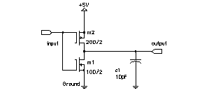
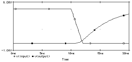
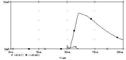
13.10.1 A PSpice ExampleFigure 13.2 shows the schematic for the output section of a CMOS I/O buffer driving a 10 pF output capacitor representing an off-chip load. The PSpice input file that follows is called a deck (from the days of punched cards): VIN input Ground PWL(0us 5V 10ns 5V 12ns 0V 20ns 0V) m1 output input Ground Ground NMOS W=100u L=2u m2 output input +5V +5V PMOS W=200u L=2u .model nmos nmos level=2 vto=0.78 tox=400e-10 nsub=8.0e15 xj=-0.15e-6 + ld=0.20e-6 uo=650 ucrit=0.62e5 uexp=0.125 vmax=5.1e4 neff=4.0 + delta=1.4 rsh=37 cgso=2.95e-10 cgdo=2.95e-10 cj=195e-6 cjsw=500e-12 .model pmos pmos level=2 vto=-0.8 tox=400e-10 nsub=6.0e15 xj=-0.05e-6 + ld=0.20e-6 uo=255 ucrit=0.86e5 uexp=0.29 vmax=3.0e4 neff=2.65 + delta=1 rsh=125 cgso=2.65e-10 cgdo=2.65e-10 cj=250e-6 cjsw=350e-12 Figure 13.3 shows the input and output waveforms as well as the current flowing in the devices.We can quickly check our circuit simulation results as follows. The total charge transferred to the 10 pF load capacitor as it charges from 0 V to 5 V is 50 pC (equal to 5 V ¥ 10 pF). This total charge should be very nearly equal to the integral of the drain current of the pull-up ( p -channel) transistor I L ( m2 ). We can get a quick estimate of the integral of the current by approximating the area under the waveform for id(m2) in Figure 13.3 as a triangle—half the base (about 12 ns) multiplied by the height (about 8 mA), so that Notice that the two estimates for the transferred charge are equal.
Next, we can check the time derivative of the pull-up current. (We can also do this by using the Probe program and requesting a plot of did(m2) ; the symbol dn represents the time derivative of quantity n for Probe. The symbol id(m2) requests Probe to plot the drain current of m2 .) The maximum derivative should be roughly equal to the maximum change of the drain current ( D I L ( m 2) = 8 mA) divided by the time taken for that change (about D t = 2 ns from Figure 13.3 ) or The large time derivative of the device current, here 4 MAs –1 , causes problems in high-speed CMOS I/O. This sharp change in current must flow in the supply leads to the chip, and through the inductance associated with the bonding wires to the chip which may be of the order of 10 nanohenrys. An electromotive force (emf ), V P , will be generated in the inductance as follows, The result is a glitch in the power supply voltage during the buffer output transient. This is known as supply bounce or ground bounce . To limit the amount of bounce we may do one of two things: We can work on the first solution by careful design of the packages and by using parallel bonding wires (inductors add in series, reduce in parallel). 13.10.2 SPICE ModelsTable 13.14 shows the SPICE parameters for the typical 0.5 m m CMOS process (0.6 m m drawn gate length), G5, that we used in Section 2.1 . These LEVEL = 3 parameters may be used with Spice3, PSpice, and HSPICE (see also Table 2.1 and Figure 2.4 ).
There are several levels of the SPICE MOSFET models, the following is a simplified overview (a huge number of confusing variations, fixes, and options have been added to these models—see Meta Software’s HSPICE User’s Manual, Vol. II, for a comprehensive description [ 1996]):
Table 13.15 shows the BSIM1 parameters (in the PSpice LEVEL = 4 format) for the G5 process. The Berkeley short-channel IGFET model ( BSIM ) family models capacitance in terms of charge. In Sections 2.1 and 3.2 we treated the gate–drain capacitance, C GD , for example, as if it were a reciprocal capacitance , and could be written assuming there was charge associated with the gate, Q G , and the drain, Q D , as follows: Equation 13.31 (the Meyer model ) would be true if the gate and drain formed a parallel plate capacitor and Q G = – Q D , but they do not. In general, Q G ≠ – Q D and Eq. 13.31 is not true. In an MOS transistor we have four regions of charge: Q G (gate), Q D (channel charge associated with the drain), Q S (channel charge associated with the drain), and Q B (charge in the bulk depletion region). These charges are not independent, since We can form a 4 ¥ 4 matrix, M , whose entries are ∂ Q i /∂ V j , where V j = V G , V S , V D , and V B . Then C ii = M ii are the terminal capacitances; and C ij = – M ij , where i ≠ j , is a transcapacitance . Equation 13.32 forces the sum of each column of M to be zero. Since the charges depend on voltage differences, there are only three independent voltages ( V GB , V DB , and V SB , for example) and each row of M must sum to zero. Thus, we have nine (= 16 – 7) independent entries in the matrix M . In general, C ij is not necessarily equal to C ji . For example, using PSpice and a LEVEL = 4 BSIM model, there are nine independent partial derivatives, printed as follows: Derivatives of gate (dQg/dVxy) and bulk (dQb/dVxy) charges From these derivatives we may compute six nonreciprocal capacitances : and three terminal capacitances: Nonreciprocal transistor capacitances cast a cloud over our analysis of gate capacitance in Section 3.2, but the error we made in neglecting this effect is small compared to the approximations we made in the sections that followed. Even though we now find the theoretical analysis was simplified, the conclusions in our treatment of logical effort and delay modeling are still sound. Sections 7.3 and 9.2 in the book on transistor modeling by Tsividis [ 1987] describe nonreciprocal capacitance in detail. Pages 15-42 to 15-44 in Vol. II of Meta Software’s HSPICE User Manual [ 1996] also gives an explanation of transcapacitance. 1. Meta Software’s HSPICE User’s Manual [ 1996], p. 15-36 and pp.16-13 to 16-15, explains these parameters. [ Chapter start ] [ Previous page ] [ Next page ] | |||||||||||||||||||||||||||||||||||||||||||||||||||||||||||||||||||||||||||||||||||||||||||||||||||||||||||||||||||||||||||||||||||||||||||||||||||||||||||||||||||||||||||||||||||||||||||||||||||||||||||||||||||||||||||||||||||||||||||||||||||||||||||||||||||||||||||||||||||||||||||||||||||||||||||||||||||||||||||||||||||||||||||||||||||||||||||||


