|
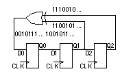
[ Chapter start ] [ Previous page ] [ Next page ] 14.7 Built-in Self-testThe trend to include more test logic on an ASIC has already been mentioned. Built-in self-test ( BIST ) is a set of structured-test techniques for combinational and sequential logic, memories, multipliers, and other embedded logic blocks. In each case the principle is to generate test vectors, apply them to the circuit under test ( CUT ) or device under test ( DUT ), and then check the response. 14.7.1 LFSRFigure 14.23 shows a linear feedback shift register ( LFSR ). The exclusive-OR gates and shift register act to produce a pseudorandom binary sequence ( PRBS ) at each of the flip-flop outputs. By correctly choosing the points at which we take the feedback from an n -bit shift register (see Section 14.7.5 ), we can produce a PRBS of length 2 n – 1, a maximal-length sequence that includes all possible patterns (or vectors) of n bits, excluding the all-zeros pattern.
Table 14.10 shows the maximal-length sequence, with length 2 3 – 1 = 7, for the 3-bit LFSR shown in Figure 14.23 . Notice that the first (clock tick 1) and last rows (clock tick 8) are identical. Rows following the seventh row repeat rows 1–7, so that the length of this 3-bit LFSR sequence is 7 = 2 3 – 1, the maximal length. The shaded regions show how bits are shifted from one clock cycle to the next. We assume the register is initialized to the all-ones state, but any initial state will work and produce the same PRBS, as long as the initial state is not all zeros (in which case the LFSR will stay stuck at all zeros).
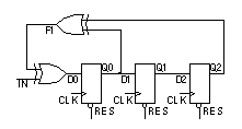
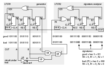
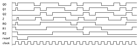
14.7.2 Signature AnalysisFigure 14.24 shows the LFSR of Figure 14.23 with an additional XOR gate used in the first stage of the shift register. If we apply a binary input sequence to IN , the shift register will perform data compaction (or compression ) on the input sequence. At the end of the input sequence the shift-register contents, Q0Q1Q2 , will form a pattern that we call a signature . If the input sequence and the serial-input signature register ( SISR ) are long enough, it is unlikely (though possible) that two different input sequences will produce the same signature. If the input sequence comes from logic that we wish to test, a fault in the logic will cause the input sequence to change. This causes the signature to change from a known good value and we shall then know that the circuit under test is bad. This technique, called signature analysis , was developed by Hewlett-Packard to test equipment in the field in the late 1970s. 14.7.3 A Simple BIST ExampleWe can combine the PRBS generator of Figure 14.23 together with the signature register of Figure 14.24 to form the simple BIST structure shown in Figure 14.25 (a). LFSR1 generates a maximal-length (2 3 – 1 = 7 cycles) PRBS. LFSR2 computes the signature ('011' for the good circuit) of the CUT. LFSR1 is initialized to '100' (Q0 = 1, Q1 = 0, Q2 = 0) and LFSR2 is initialized to '000'. The schematic in Figure 14.25 (a) shows the bit sequences in the circuit, both for a good circuit and for a bad circuit with a stuck-at-1 fault, F1. Figure 14.25 (b) shows how the bit sequences are calculated in the good circuit. The signature is formed as R0R1R2 seven clock edges (on the eighth clock cycle) after the active-low reset is taken high. Figure 14.26 shows the waveforms in the good and bad circuit. The bad circuit signature, '000', differs from the good circuit and the signature can either be compared with the known good signature on-chip or the signature may be shifted out and compared off-chip (both approaches are used in practice).
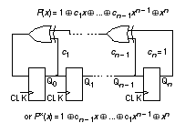
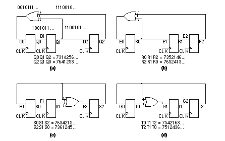
14.7.4 AliasingIn Figure 14.26 the good and bad circuits produced different signatures. There is a small probability that the signature of a bad circuit will be the same as a good circuit. This problem is known as aliasing or error masking . For the example in Figure 14.25 , the bit stream input to the signature analysis register is 7 bits long. There are 2 7 or 128 possible 7-bit-long bit-stream patterns. We assume that each of these 128 bit-stream patterns is equally likely to produce any of the eight (all-zeros is an allowed pattern in a signature register) possible 3-bit signatures. It turns out that this is a good assumption. Thus there are 128 / 8 or 16 bit-streams that produce the good signature, one of these belongs to the good circuit, the remaining 15 cause aliasing. Since there are a total of 128 – 1 = 127 bit-streams due to bad circuits, the fraction of bad-circuit bit-streams that cause aliasing is 15 / 127, or 0.118. If all bad circuit bit-streams are equally likely (and this is a poor assumption) then 0.118 is also the probability of aliasing. In general, if the length of the test sequence is L and the length of the signature register is R the probability p of aliasing (not detecting an error) is Thus, for the example in Figure 14.25 , L = 7 and R = 3, and the probability of aliasing is p = (2 (7 – 3) – 1) / (2 7 – 1) = 15 / 127 = 0.118, as we have just calculated. This is a very high probability of error and we would not use such a short test sequence and such a short signature register in practice. For L >> R the error probability is For example, if R = 16, p ª 0.0000152 corresponding to an error coverage (1 – p ) of approximately 99.9984 percent. Unfortunately, these equations for error coverage are rather meaningless since there is no easy way to relate the error coverage to fault coverage. The problem lies in our assumption that all bad-circuit bit-streams are equally likely, and this is not true in practice (for example, bit-stream outputs of all ones or all zeros are more likely to occur as a result of faults). Nevertheless signature analysis with high error-coverage rates is found to produce high fault coverage. 14.7.5 LFSR TheoryThe operation of LFSRs is related to the mathematics of polynomials and Galois-field theory. The properties and behavior of these polynomials are well known and they are also used extensively in coding theory. Every LFSR has a characteristic polynomial that describes its behavior. The characteristic polynomials that cause an LFSR to generate a maximum-length PRBS are called primitive polynomials. Consider the primitive polynomial where a ⊕ b represents the exclusive-OR of a and b . The order of this polynomial is three, and the corresponding LFSR will generate a PRBS of length 2 3 – 1 = 7. For a primitive polynomial of order n , the length of the PRBS is 2 n – 1. Figure 14.27 shows the nonzero coefficients of some primitive polynomials [ Golomb et al., 1982]. Any primitive polynomial can be written as where c 0 and c n are always one. Thus for example, from Figure 14.27 for n = 3, we see s = 0, 1, 3; and thus the nonzero coefficients are c 0 , c 1 , and c 3 . This corresponds to the primitive polynomial P(x) = 1 ⊕ x 1 ⊕ x 3 . There is no easy way to determine the coefficients of primitive polynomials, especially for large n . There are many primitive polynomials for each n , but Figure 14.27 lists the one with the fewest nonzero coefficients. The schematic in Figure 14.27 shows how the feedback taps on a LFSR correspond to the nonzero coefficients of the primitive polynomial. If the i th coefficient c i is 1, then we include a feedback connection and an XOR gate in that position. If c i is zero, there is no feedback connection and no XOR gate in that position. The reciprocal of a primitive polynomial, P*(x) , is also primitive, where For example, by taking the reciprocal of the primitive polynomial P(x) = 1 ⊕ x 1 ⊕ x 3 from Eq. 14.17 , we can form which is also a primitive polynomial. This means that there are two possible LFSR implementations for every P(x) . Or, looked at another way, for every LFSR implementation, the characteristic polynomial can be written in terms of two primitive polynomials, P(x) and P*(x) , that are reciprocals of each other. We may also implement an LFSR by using XOR gates in series with each flip-flop output rather than external to the shift register. The external-XOR LFSR is called a type 1 LFSR and the internal-XOR LFSR is called a type 2 LFSR (this is a nomenclature that most follow). Figure 14.28 shows the four different LFSRs that may be constructed for each primitive polynomial, P(x) . There are differences between the four different LFSRs for each polynomial. Each gives a different output sequence. The outputs for the type 1 LFSRs, taken from the Q outputs of each flip-flop, are identical, but delayed by one clock cycle from the previous output. This is a problem when we use the parallel output from an LFSR to test logic because of the strong correlation between the test signals. The type 2 LFSRs do not have this problem. The type 2 LFSRs also are capable of higher-frequency operation since there are fewer series XOR gates in the signal path than in the corresponding type 1 LFSR. For these reasons, the type 2 LFSRs are usually used in BIST structures. The type 1 LFSR does have the advantage that it can be more easily constructed using register structures that already exist on an ASIC. Table 14.11 shows primitive polynomial coefficients for higher values of n than Figure 14.27 . Test length grows quickly with the size of the LFSR. For example, a 32-bit generator will produce a sequence with 2 32 = 4,294,967,296 ª 4.3 ¥ 10 9 bits. With a 100 MHz clock (with 10 ns cycle time), the test time of 43 seconds would be impractical.
There is confusion over naming, labeling, and drawing of LFSRs in texts and test programs. Looking at the schematic in Figure 14.27 , we can draw the LFSR with signals flowing from left to right or vice versa (two ways), we can name the leftmost flip-flop output Q 0 or Q n (two more ways), and we can name the coefficient that goes with Q 0 either c 0 or c n – 1 (two more ways). There are thus at least 2 3 ¥ 4 different ways to draw an LFSR for a given polynomial. Four of these are distinct. You can connect the LFSR feedback in the reverse order and the LFSR will still work—you will, however, get a different sequence. Usually this does not matter. 14.7.6 LFSR ExampleWe can use a cell compiler to produce LFSR and signature register BIST structures. For example, we might complete a property sheet as follows: property name value property name value ------------------ ----- ------------------ ----- LFSR_is_bilbo false LFSR_configuration generator LFSR_length 3 LFSR_init_hex_value 4 LFSR_scan false LFSR_mux_data false LFSR_mux_output false LFSR_xor_hex_function max_length LFSR_zero_state false LFSR_signature_inputs 1 The Verilog structural netlist for the compiled type 2 LFSR generator is shown in Table 14.12 . According to our notation and the primitive polynomials in Figure 14.27 , the corresponding primitive polynomial is P*(x) = 1 ⊕ x 2 ⊕ x 3 . The LFSR has both serial and parallel outputs (taken from the inverted flip-flop outputs with inverting buffers, cell names in02d1 ). The clock and reset inputs are buffered (with noninverting buffers, cell names ni01d1 ) since these inputs would normally have to drive a load of more than 3 bits. Looking in the cell data book we find that the flip-flop corresponding to the MSB, instance FF0 with cell name dfptnb , has an active-low set input SDN . The remaining flip-flops, cell name dfctnb , have active-low clears, CDN . This gives us the initial value '100'. Table 14.13 shows the serial-input signature register compiled using the reciprocal polynomial. Again the compiler has included buffers. All the flip-flops, cell names dfctnb , have active-low clear so that the initial content of the register is '000'. 14.7.7 MISRA serial-input signature register can only be used to test logic with a single output. We can extend the idea of a serial-input signature register to the multiple-input signature register ( MISR ) shown in Figure 14.29 . There are several ways to connect the inputs to both types (type 1 and type 2) of LFSRs to form an MISR. Since the XOR operation is linear and associative, so that ( A ⊕ B) ⊕ C = A ⊕ (B ⊕ C ), as long as the result of the additions are the same then the different representations are equivalent. If we have an n -bit long MISR we can accommodate up to n inputs to form the signature. If we use m < n inputs we do not need the extra XOR gates in the last n – m positions of the MISR.
There are several types of BIST architecture based on the MISR. By including extra logic we can reconfigure an MISR to be an LFSR or a signature register; this is called a built-in logic block observer ( BILBO ). By including the logic that we wish to test in the feedback path of an MISR, we can construct circular BIST structures. One of these is known as the circular self-test path ( CSTP ). We can test compiled blocks including RAM, ROM, and datapath elements using an LFSR generator and a MISR. To generate all 2 n address values for a RAM or ROM we can modify the LFSR feedback path to force entrance and exit from the all-zeros state. This is known as a complete LFSR . The pattern generator does not have to be an LFSR or exhaustive. For example, if we were to apply an exhaustive test to a 4-bit by 4-bit multiplier this would require 2 8 or 256 vectors. An 8-bit by 8-bit multiplier requires 65,536 vectors and, if it were possible to test a 32-bit by 32-bit multiplier exhaustively, it would require 1.8 ¥ 10 19 vectors. Table 14.14 shows two sets of nonexhaustive test patterns, {SA} and {SAE}, if A and B are both 4 bits wide. The test sequences {SA} and {SAE} consist of nested sequences of walking 1’s and walking 0’s (S1 and S1B), walking pairs (S2 and S2B), and triplets (S3, S3B). The sequences are extended for larger inputs, so that, for example, {S2} is a sequence of seven vectors for an 8-bit input and so on. Intermediate sequences {SX} and {SXB} are concatenated from S1, S2, and S3; and from S1B, S2B, and S3B respectively. These sequences are chosen to exercise as many of the add-and-carry functions within the multiplier as possible.
The sequence length of {SA} is 3A (B – 1), and 3(2A – 1)(3B – 2) for {SAE}, where A and B are the sizes of the multiplier inputs. For example, {SA} is 168 vectors for A = B = 8 and 2976 vectors for A = B = 32; {SAE} is 990 vectors (A = B = 8) and 17,766 vectors (A = B = 32). From fault simulation, the stuck-at fault coverage is 93 percent for sequence {SA} and 97 percent for sequence {SAE}. Figure 14.30 shows an MISR with a scan chain. We can now include the BIST logic as part of a boundary-scan chain, this approach is called scanBIST .
[ Chapter start ] [ Previous page ] [ Next page ] | ||||||||||||||||||||||||||||||||||||||||||||||||||||||||||||||||||||||||||||||||||||||||||||||||||||||||||||||||||||||||||||||||||||||||||||||||||||||||||||||||||||||||||||||||||||||||||||||||||||||||||||||||||||||||||||

