|
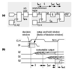
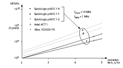
[ Chapter start ] [ Previous page ] [ Next page ] 6.4 AC InputSuppose we wish to connect an input bus containing sampled data from an analog-to-digital converter ( A/D ) that is running at a clock frequency of 100 kHz to an FPGA that is running from a system clock on a bus at 10 MHz (a NuBus). We are to perform some filtering and calculations on the sampled data before placing it on the NuBus. We cannot just connect the A/D output bus to our FPGA, because we have no idea when the A/D data will change. Even though the A/D data rate (a sample every 10 m s or every 100 NuBus clock cycles) is much lower than the NuBus clock, if the data happens to arrive just before we are due to place an output on the NuBus, we have no time to perform any calculations. Instead we want to register the data at the input to give us a whole NuBus clock cycle (100 ns) to perform the calculations. We know that we should have the A/D data at the flip-flop input for at least the flip-flop setup time before the NuBus clock edge. Unfortunately there is no way to guarantee this; the A/D converter clock and the NuBus clock are completely independent. Thus it is entirely possible that every now and again the A/D data will change just before the NuBus clock edge. 6.4.1 MetastabilityIf we change the data input to a flip-flop (or a latch) too close to the clock edge (called a setup or hold-time violation ), we run into a problem called metastability , illustrated in Figure 6.16. In this situation the flip-flop cannot decide whether its output should be a '1' or a '0' for a long time. If the flip-flop makes a decision, at a time t r after the clock edge, as to whether its output is a '1' or a '0', there is a small, but finite, probability that the flip-flop will decide the output is a '1' when it should have been a '0' or vice versa. This situation, called an upset , can happen when the data is coming from the outside world and the flip-flop can’t determine when it will arrive; this is an asynchronous signal , because it is not synchronized to the chip clock. Experimentally we find that the probability of upset , p , is (per data event, per clock edge, in one second, with units Hz –1 ·Hz –1 ·s –1 ) where t r is the time a sampler (flip-flop or latch) has to resolve the sampler output; T 0 and t c are constants of the sampler circuit design. Let us see how serious this problem is in practice. If t r = 5 ns, t c = 0.1 ns, and T 0 = 0.1 s, Eq. 6.2 gives the upset probability as which is very small, but the data and clock may be running at several MHz, causing the sampler plenty of opportunities for upset. The mean time between upsets ( MTBU , similar to MTBF—mean time between failures) is where f clock is the clock frequency and f data is the data frequency. If t r = 5 ns, t c = 0.1 ns, T 0 = 0.1 s (as in the previous example), f clock = 100 MHz, and f data = 1 MHz, then or about 16 years (10 8 seconds is three years, and a day is 10 5 seconds). An MTBU of 16 years may seem safe, but suppose we have a 64-bit input bus using 64 flip-flops. If each flip-flop has an MTBU of 16 years, our system-level MTBF is three months. If we ship 1000 systems we would have an average of 10 systems failing every day. What can we do? The parameter t c is the inverse of the gain–bandwidth product , GB , of the sampler at the instant of sampling. It is a constant that is independent of whether we are sampling a positive or negative data edge. It may be determined by a small-signal analysis of the sampler at the sampling instant or by measurement. It cannot be determined by simulating the transient response of the flip-flop to a metastable event since the gain and bandwidth both normally change as a function of time. We cannot change t c . The parameter T 0 (units of time) is a function of the process technology and the circuit design. It may be different for sampling a positive or negative data edge, but normally only one value of T 0 is given. Attempts have been made to calculate T 0 and to relate it to a physical quantity. The best method is by measurement or simulation of metastable events. We cannot change T 0 . Given a good flip-flop or latch design, t c and T 0 should be similar for comparable CMOS processes (so, for example, all 0.5 m m processes should have approximately the same t c and T 0 ). The only parameter we can change when using a flip-flop or latch from a cell library is t r , and we should allow as much resolution time as we can after the output of a latch before the signal is clocked again. If we use a flip-flop constructed from two latches in series (a master–slave design), then we are sampling the data twice. The resolution time for the first sample t r is fixed, it is half the clock cycle (if the clock is high and low for equal times—we say the clock has a 50 percent duty cycle , or equal mark–space ratio ). Using such a flip-flop we need to allow as much time as we can before we clock the second sample by connecting two flip-flops in series, without any combinational logic between them, if possible. If you are really in trouble, the next step is to divide the clock so you can extend the resolution time even further. Table 6.2 shows flip-flop metastability parameters and Figure 6.17 graphs the metastability data for f clock = 10 MHz and f data = 1 MHz. From this graph we can see the enormous variation in MTBF caused by small variations in t c . For example, in the QuickLogic pASIC 1 series the range of T 0 from 0.3 to 1.2 ¥ 10 –10 s is 4:1, but it is the range of t c = 0.2 – 0.3 ns (a variation of only 1:1.5) that is responsible for the enormous variation in MTBF (nearly four orders of magnitude at t r = 5 ns). The variation in t c is caused by the variation in GB between the QuickLogic speed grades. Variation in the other vendors’ parts will be similar, but most vendors do not show this information. To be safe, build a large safety margin for MTBF into any design—it is not unreasonable to use a margin of four orders of magnitude.
Some cell libraries include a synchronizer , built from two flip-flops in cascade, that greatly reduces the effective values of t c and T 0 over a single flip-flop. The penalty is an extra clock cycle of latency. To compare discrete TTL parts with ASIC flip-flops, the 74AS4374 TTL metastable-hardened dual flip-flops , from TI, have t c = 0.42 ns and T 0 = 4 ns. The parameter T 0 ranges from about 10 s for the 74LS74 (a regular flip-flop) to 4 ns for the 74AS4374 (over nine orders of magnitude different); t c only varies from 0.42 ns (74AS374) to 1.3 ns (74LS74), but this small variation in t c is just as important. [ Chapter start ] [ Previous page ] [ Next page ] | |||||||||||||||||||||||||||||||||||||||||||||||||||||||||||||||||||


