|
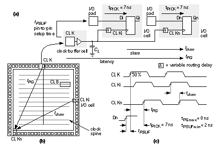
[ Chapter start ] [ Previous page ] [ Next page ] 6.5 Clock InputWhen we bring the clock signal onto a chip, we may need to adjust the logic level (clock signals are often driven by TTL drivers with a high current output capability) and then we need to distribute the clock signal around the chip as it is needed. FPGAs normally provide special clock buffers and clock networks. We need to minimize the clock delay (or latency), but we also need to minimize the clock skew. 6.5.1 Registered InputsSome FPGAs provide a flip-flop or latch that you can use as part of the I/O circuit (registered I/O). For other FPGAs you have to use a flip-flop or latch using the basic logic cell in the core. In either case the important parameter is the input setup time. We can measure the setup with respect to the clock signal at the flip-flop or the clock signal at the clock input pad. The difference between these two parameters is the clock delay. Figure 6.18 shows part of the I/O timing model for a Xilinx XC40005-6. 1
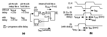
To calculate the flip-flop setup time ( t PSUFmin ) relative to the clock pad (which is the parameter system designers need to know), we subtract the clock delay, so that The problem is that we cannot easily calculate t PG , since it depends on the clock distribution scheme and where the flip-flop is on the chip. Instead Xilinx specifies t PSUFmin directly, measured from the data pad to the clock pad; this time is called a pin-to-pin timing parameter . Notice t PSUF min = 2 ns ≠ t PICK – t PG max = –1 ns. Figure 6.19 shows that the hold time for a XC4005-6 flip-flop ( t CKI ) with respect to the flip-flop clock is zero. However, the pin-to-pin hold time including the clock delay is t PHF = 5.5 ns. We can remove this inconvenient hold-time restriction by delaying the input signal. Including a programmable delay allows Xilinx to guarantee the pin-to-pin hold time ( t PH ) as zero. The penalty is an increase in the pin-to-pin setup time ( t PSU ) to 21 ns (from 2 ns) for the XC4005-6, for example.
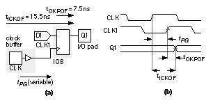
We also have to account for clock delay when we register an output. Figure 6.20 shows the timing model diagram for the clock-to-output delay.
[ Chapter start ] [ Previous page ] [ Next page ] | ||||||


