|
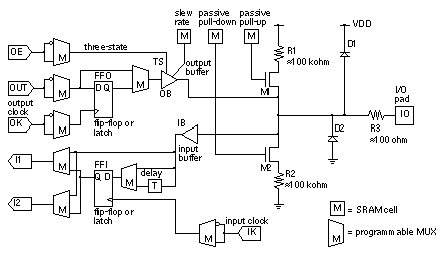
[ Chapter start ] [ Previous page ] [ Next page ] 6.7 Xilinx I/O BlockThe Xilinx I/O cell is the input/output block ( IOB ) . Figure 6.21 shows the Xilinx XC4000 IOB, which is similar to the IOB in the XC2000, XC3000, and XC5200 but performs a superset of the options in these other Xilinx FPGAs.
The outputs contain features that allow you to do the following:
The features on the inputs allow you to do the following:
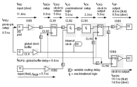
Figure 6.22 shows the timing model for the XC5200 family. 1 It is similar to the timing model for all the other Xilinx LCA FPGAs with one exception—the XC5200 does not have registers in the I/O cell; you go directly to the core CLBs to include a flip-flop or latch on an input or output. 6.7.1 Boundary ScanTesting PCBs can be done using a bed-of-nails tester. This approach becomes very difficult with closer IC pin spacing and more sophisticated assembly methods using surface-mount technology and multilayer boards. The IEEE implemented boundary-scan standard 1149.1 to simplify the problem of testing at the board level. The Joint Test Action Group (JTAG) developed the standard; thus the terms JTAG boundary scan or just JTAG are commonly used. Many FPGAs contain a standard boundary-scan test logic structure with a four-pin interface. By using these four signals, you can program the chip using ISP, as well as serially load commands and data into the chips to control the outputs and check the inputs. This is a great improvement over bed-of-nails testing. We shall cover boundary scan in detail in Section 14.6, “Scan Test.” [ Chapter start ] [ Previous page ] [ Next page ] | ||


