7.2
Xilinx LCA
Figure 7.5
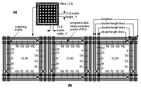
shows the hierarchical Xilinx LCA interconnect architecture.
-
The
vertical lines and
horizontal lines run between CLBs.
-
The
general-purpose interconnect joins
switch boxes (also known as
magic boxes or
switching matrices).
-
The
long lines run across the entire chip. It is possible to form internal buses using long lines and the three-state buffers that are next to each CLB.
-
The
direct connections (not used on the XC4000) bypass the switch matrices and directly connect adjacent CLBs.
-
The
Programmable Interconnection Points (
PIP
s) are programmable pass transistors that connect the CLB inputs and outputs to the routing network.
-
The
bidirectional (
BIDI
) interconnect buffers restore the logic level and logic strength on long interconnect paths.
|
|
|
FIGURE 7.5
Xilinx LCA interconnect. (a) The LCA architecture (notice the matrix element size is larger than a CLB). (b) A simplified representation of the interconnect resources. Each of the lines is a bus.
|
Table 7.3
shows the interconnect data for an XC3020, a typical Xilinx LCA FPGA, that uses two-level metal interconnect.
Figure 7.6
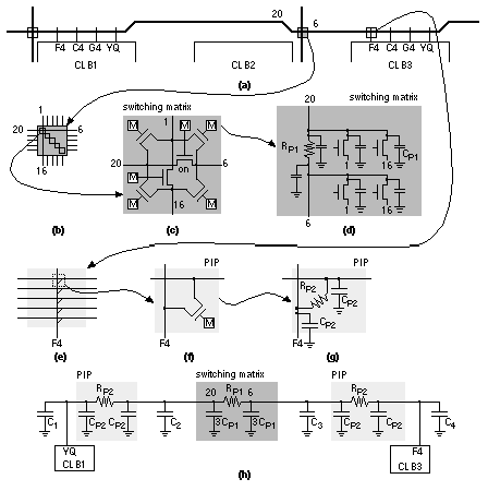
shows the switching matrix. Programming a switch matrix allows a number of different connections between the general-purpose interconnect.
|
TABLE 7.3
XC3000 interconnect parameters.
|
|
Parameter
|
XC3020
|
|
Technology
|
1.0
m
m,
l
= 0.5
m
m
|
|
Die height
|
220 mil
|
|
Die width
|
180 mil
|
|
Die area
|
39,600 mil
2
= 102 M
l
2
|
|
CLB matrix height (Y)
|
480
m
m = 960
l
|
|
CLB matrix width (X)
|
370
m
m = 740
l
|
|
CLB matrix area (X
¥
Y)
|
17,600
m
m
2
= 710 k
l
2
|
|
Matrix transistor resistance, R
P1
|
0.5–1k
W
|
|
Matrix transistor parasitic capacitance, C
P1
|
0.01–0.02 pF
|
|
PIP transistor resistance, R
P2
|
0.5–1k
W
|
|
PIP transistor parasitic capacitance, C
P2
|
0.01–0.02 pF
|
|
Single-length line (X, Y)
|
370
m
m, 480
m
m
|
|
Single-length line capacitance: C
LX
, C
LY
|
0.075 pF, 0.1 pF
|
|
Horizontal Longline (8X)
|
8 cols. = 2960
m
m
|
|
Horizontal Longline metal capacitance, C
LL
|
0.6 pF
|
In
Figure 7.6
(d), (g), and (h):
|
|
|
FIGURE 7.6
Components of interconnect delay in a Xilinx LCA array. (a) A portion of the interconnect around the CLBs. (b) A switching matrix. (c) A detailed view inside the switching matrix showing the pass-transistor arrangement. (d) The equivalent circuit for the connection between nets 6 and 20 using the matrix. (e) A view of the interconnect at a Programmable Interconnection Point (PIP). (f) and (g) The equivalent schematic of a PIP connection. (h) The complete RC delay path.
|
-
C1
=
3CP1
+
3CP2
+ 0.
5C
LX
is the parasitic capacitance due to the switch matrix and PIPs (F4, C4, G4) for CLB1, and half of the line capacitance for the double-length line adjacent to CLB1.
-
C
P1
and
R
P1
are the switching-matrix parasitic capacitance and resistance.
-
C
P2
and
R
P2
are the parasitic capacitance and resistance for the PIP connecting YQ of CLB1 and F4 of CLB3.
-
C2
= 0.
5CLX
+
CLX
accounts for half of the line adjacent to CLB1 and the line adjacent to CLB2.
-
C
3
= 0.
5C
LX
accounts for half of the line adjacent to CLB3.
-
C
4
= 0.
5C
LX
+
3C
P2
+
C
LX
+
3C
P1
accounts for half of the line adjacent to CLB3, the PIPs of CLB3 (C4, G4, YQ), and the rest of the line and switch matrix capacitance following CLB3.
We can determine Elmore’s time constant for the connection shown in
Figure 7.6
as
|
t
D
|
=
|
R
P2
(C
P2
+ C
2
+ 3C
P1
) + (R
P2
+ R
P1
)(3C
P1
+ C
3
+ C
P2
)
|
(7.9)
|
|
|
|
+ (2R
P2
+ R
P1
)(C
P2
+ C
4
) .
|
|
If
RP1
=
RP2
, and
CP1
=
CP2
, then
|
t
D
|
=
|
(15 + 21)R
P
C
P
+ (1.5 + 1 + 4.5)R
P
C
LX
.
|
(7.10)
|
We need to know the pass-transistor resistance
RP
. For example, suppose
RP
= 1k
W
. If  k
'
n
= 50
m
AV
–2
, then (with
Vt
n
= 0.65 V and
V
DD
= 3.3 V)
|
|
|
1
|
|
1
|
|
|
|
|
W/L
|
=
|
––––––––––
|
=
|
––––––––––––––––––––––––––
|
=
|
7.5 .
|
(7.11)
|
|
|
|
k
'
n
R
p
(
V
DD
– V
t
n
)
|
|
(50
¥
10
–6
)(1
¥
10
3
)(3.3 – 0.65)
|
|
|
|
If L = 1
m
m, both source and drain areas are 7.5
m
m long and approximately 3
m
m wide (determined by diffusion overlap of contact, contact width, and contact-to-gate spacing, rules 6.1a + 6.2a + 6.4a = 5.5
l
in
Table 2.7
). Both drain and source areas are thus 23
m
m
2
and the sidewall perimeters are 14
m
m (excluding the sidewall facing the channel). If we have a diffusion capacitance of 140 aF
m
m
–2
(area) and 500 aF
m
m
–1
(perimeter), typical values for a 1.0
m
m process, the parasitic source and drain capacitance is
|
C
P
|
=
|
(140
¥
10
–18
)(23) + (500
¥
10
–18
)(14)
|
(7.12)
|
|
|
=
|
1.022
¥
10
–14
F .
|
|
If we assume
CP
= 0.01 pF and
CLX
= 0.075 pF (
Table 7.3
),
|
t
D
|
=
|
(36)(1)(0.01) + (7)(1)(0.075)
|
(7.13)
|
|
|
=
|
0.885 ns .
|
|
A delay of approximately 1 ns agrees with the typical values from the XACT delay calculator and is about the fastest connection we can make between two CLBs.
|
|
|
FIGURE 7.7
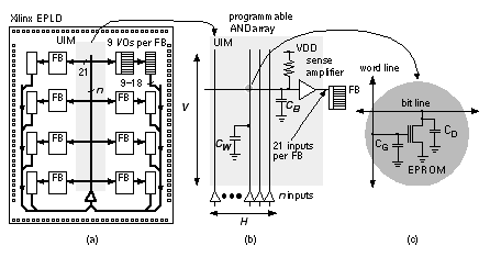
The Xilinx EPLD UIM (Universal Interconnection Module). (a) A simplified block diagram of the UIM. The UIM bus width,
n
, varies from 68 (XC7236) to 198 (XC73108). (b) The UIM is actually a large programmable AND array. (c) The parasitic capacitance of the EPROM cell.
|
[ Chapter start ] [ Previous page ] [ Next page ] | 


 k
'
n
= 50


