|
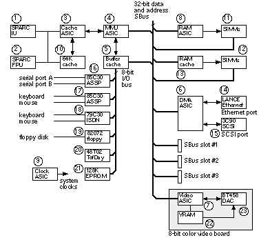
[ Chapter start ] [ Previous page ] [ Next page ] 15.3 System PartitioningMicroelectronic systems typically consist of many functional blocks. If a functional block is too large to fit in one ASIC, we may have to split, or partition, the function into pieces using goals and objectives that we need to specify. For example, we might want to minimize the number of pins for each ASIC to minimize package cost. We can use CAD tools to help us with this type of system partitioning. Figure 15.2 shows the system diagram of the Sun Microsystems SPARCstation 1. The system is partitioned as follows; the numbers refer to the labels in Figure 15.2 . (See Section 1.3, “Case Study” for the sources of infomation in this section.)
Table 15.1 shows the details of the nine custom ASICs used in the SPARCstation 1. Some of the partitioning of the system shown in Figure 15.2 is determined by whether to use ASSPs or custom ASICs. Some of these design decisions are based on intangible issues: time to market, previous experience with a technology, the ability to reuse part of a design from a previous product. No CAD tools can help with such decisions. The goals and objectives are too poorly defined and finding a way to measure these factors is very difficult. CAD tools cannot answer a question such as: “What is the cheapest way to build my system?” but can help the designer answer the question: “How do I split this circuit into pieces that will fit on a chip?” Table 15.2 shows the partitioning of the SPARCstation 10 so you can compare it to the SPARCstation 1. Notice that the gate counts of nearly all of the SPARCstation 10 ASICs have increased by a factor of 10, but the pin counts have increased by a smaller factor.
[ Chapter start ] [ Previous page ] [ Next page ] | |||||||||||||||||||||||||||||||||||||||||||||||||||||||||||||||||||||||||||||||||||||||||||||||||||||||||||


