16.6 Problems
16.6
Problems
* = Difficult, ** = Very difficult, *** = Extremely difficult
16.1 (Wire loads, 30 min.)
Table 16.2
shows a wire-load table. Since you might expect the interconnect load to be a monotonic increasing function of fanout and block area, it seems as though some of the data in
Table 16.2
may be in error; these figures are shown preceded by an asterisk, '*' (this table is from an ASIC vendor data book). Using a spreadsheet, analyze the data in
Table 16.2
.
-
a. By graphing the data, indicate any figures in
Table 16.2
that you think might be in error. If you think that there is an error, predict the correct values—either by interpolation (for values in error in the body of the table), or by fitting the linear model parameters, the slope and the intercept (for any values in error in the last two columns of the table).
-
b. Including any corrections, how accurate is the model that predicts load as a linear function of fanout for a given block size? (Use the maximum error of the linear model expressed as a percentage of the table value.)
-
c. Can you fit a simple function to the (possibly corrected) figures in the last column of the table and explain its form?
-
d. What did you learn about wire-load tables from this problem?
|
TABLE 16.2 Wire- load table. Predicted interconnect loads (measured in standard loads) as a function of block size and fanout (Problem
16.1
).
|
|
Size
(/mm
2
)
|
Fanout
|
Slope
|
Intercept
|
|
1
|
2
|
3
|
4
|
5
|
6
|
7
|
8
|
16
|
32
|
64
|
|
0.5
¥
0.5
|
0.65
|
0.95
|
1.25
|
1.54
|
1.84
|
2.14
|
2.44
|
2.74
|
5.13
|
9.91
|
19.47
|
0.299
|
0.349
|
|
1
¥
1
|
0.80
|
1.20
|
1.59
|
1.99
|
2.39
|
2.79
|
3.19
|
3.59
|
6.77
|
13.15
|
25.9
|
0.398
|
0.398
|
|
2
¥
2
|
0.96
|
1.48
|
1.99
|
2.51
|
3.02
|
3.54
|
4.05
|
4.57
|
8.68
|
16.92
|
33.38
|
0.515
|
0.448
|
|
3
¥
3
|
1.20
|
1.83
|
2.46
|
3.09
|
3.72
|
4.35
|
4.98
|
5.61
|
10.66
|
20.75
|
40.94
|
0.631
|
0.564
|
|
4
¥
4
|
1.41
|
2.11
|
2.81
|
3.50
|
4.20
|
4.90
|
5.59
|
6.29
|
11.87
|
23.02
|
45.33
|
0.697
|
0.714
|
|
5
¥
5
|
1.51
|
2.24
|
2.97
|
3.70
|
4.43
|
5.16
|
5.89
|
6.62
|
12.47
|
24.15
|
47.53
|
0.730
|
0.780
|
|
6
¥
6
|
1.56
|
2.31
|
3.05
|
3.80
|
4.55
|
5.30
|
6.04
|
6.79
|
12.77
|
24.72
|
48.62
|
0.747
|
0.813
|
|
7
¥
7
|
1.83
|
2.62
|
3.42
|
4.22
|
5.01
|
5.81
|
6.61
|
7.40
|
13.78
|
26.53
|
52.02
|
0.797
|
* 1.029
|
|
8
¥
8
|
1.88
|
2.74
|
3.6
|
4.47
|
5.33
|
6.19
|
7.06
|
7.92
|
14.82
|
26.64
|
56.26
|
0.863
|
1.013
|
|
9
¥
9
|
2.01
|
2.94
|
3.87
|
4.80
|
5.73
|
6.66
|
7.59
|
8.52
|
15.95
|
30.83
|
60.57
|
0.930
|
1.079
|
|
10
¥
10
|
2.01
|
2.98
|
3.94
|
4.90
|
5.86
|
6.83
|
7.79
|
8.75
|
16.45
|
31.86
|
62.67
|
0.963
|
* 1.050
|
|
11
¥
11
|
2.46
|
3.46
|
4.45
|
5.45
|
6.44
|
7.44
|
8.44
|
9.43
|
17.4
|
33.33
|
65.20
|
0.996
|
1.465
|
|
12
¥
12
|
3.04
|
4.1
|
5.17
|
6.23
|
7.3
|
8.35
|
9.42
|
10.48
|
18.8
|
36.03
|
70.00
|
1.063
|
1.964
|
16.2
(Trees, 20 min.) For the network graph shown in
Figure 16.32
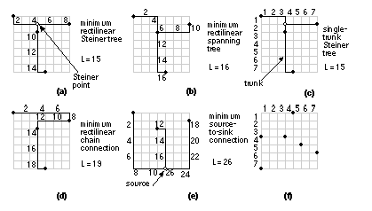
(f), draw the following trees and calculate their Manhattan lengths:
-
a. The minimum Steiner tree.
-
b. The
chain connection
.
-
c. The minimum rectilinear Steiner tree.
-
d. The
minimum rectilinear spanning tree
[
Hwang, 1976].
-
e. The minimum single-trunk rectilinear Steiner tree (with a horizontal or vertical trunk).
-
f. The
minimum rectilinear chain connection
(easy to compute).
-
g. The
minimum source-to-sink connection
.
Calculate:
-
h. The complete-graph measure and the half-perimeter measure.
Figure 16.32
parts (a–e) illustrate the definitions of these trees. There is no known solution to the minimum Steiner-tree problem for nets with more than five terminals.
|
|
|
FIGURE 16.32
Tree routing. (a) The minimum rectilinear Steiner tree (MRST). (b) The minimum rectilinear spanning tree. (c) The minimum single-trunk rectilinear Steiner tree (1-MRST). (d) The minimum rectilinear chain connection. (e) The minimum source-to-sink connection. (f) Example net for Problem
16.2
.
|
16.3
(Eigenvalue placement constraints, 10 min. [
Cheng and Kuh, 1984]) Consider the one-dimensional placement problem with a vector list of valid positions for the logic cells
p
= [
p
i
] and a vector list of
x
-coordinates for the logic cells
x
= [
x
i
].
Show that for a valid placement
x
(where the vector elements
x
i
are some permutation of the vector elements
p
i
), the following equations hold:
|
n
|
|
|
n
|
|
|
|
|
S
|
x
i
|
=
|
S
|
p
i
|
|
|
|
i
= 1
|
|
|
i
= 1
|
|
|
|
|
|
|
|
|
|
|
|
|
n
|
|
|
n
|
|
|
|
|
S
|
x
i
2
|
=
|
S
|
p
i
2
|
|
|
|
i
= 1
|
|
|
i
= 1
|
|
|
|
|
|
|
|
|
|
|
|
|
|
...
|
|
|
|
|
|
|
n
|
|
|
n
|
|
|
|
|
S
|
x
i
n
|
=
|
S
|
p
i
n
|
|
(16.22)
|
|
i
= 1
|
|
|
i
= 1
|
|
|
|
(
Hint:
Consider the polynomial (
x
+
x
i
)
n
. In our simplification to the problem, we chose to impose only the second equation of these constraints.)
16.4
(*Eigenvalue placement, 30 min.) You will need MatLab, Mathematica, or a similar mathematical calculus program for this problem.
-
a. Find the eigenvalues and eigenvectors for the disconnection matrix corresponding to the following connection matrix:
C=
[ 0 1 1 0 0 0 1 0 0;
1 0 0 0 0 0 0 0 0;
1 0 0 1 0 0 0 1 0;
0 0 1 0 0 1 0 0 0;
0 0 0 0 0 1 0 0 1;
0 0 0 1 1 0 1 0 0;
1 0 0 0 0 1 0 0 0;
0 0 1 0 0 0 0 0 1;
0 0 0 0 1 0 0 1 0;]
(
Hint:
Check your answer. The smallest, nonzero, eigenvalue should be 0.5045.)
-
b. Use your results to place the logic cells. Plot the placement and show the connections between logic cells (this is easy to do using an X-Y plot in an Excel spreadsheet).
-
c. Check that the following equation holds:
16.5
(Die size, 10 min.) Suppose the minimum spacing between pad centers is
W
mil (1 mil = 10
–3
inch), there are
N
I/O pads on a chip, and the die area (assume a square die) is
A
mil
2
:
-
a. Derive a relationship between
W
,
N
, and
A
that corresponds to the point at which the die changes from being pad-limited to core-limited.
-
b. Plot this relationship with
N
(ranging from 50 to 500 pads) on the
x
-axis,
A
on the
y
-axis (for dies ranging in size from 1 mm to 20 mm on a side), and
W
as a parameter (for
W
= 1, 2, 3, and 4 mil).
16.6
(Power buses, 20 min.) Assume aluminum metal interconnect has a resistance of about 30 m
W
/square (a low value). Consider a power ring for the I/O pads. Suppose you have a high-power chip that dissipates 5 W at
V
DD
= 5 V, and assume that half of the supply current (0.5 A) is due to I/O. Suppose the square die is
L
mil on a side, and that the I/O current is equally distributed among the
N
VDD pads that are on the chip. In the worst case, you want no more than 100 mV drop between any VDD pad and the I/O circuits drawing power (notice that there will be an equal drop on the VSS side; just consider the VDD drop).
-
a. Model the power distribution as a ring of
N
equally spaced pads. Each pad is connected by a resistor equal to the aluminum VDD power-bus resistance between two pads. Assume the I/O circuits associated with each pad can be considered to connect to just one point on the resistors between each pad. If the resistance between each pad is
R
, what is the worst-case resistance between the I/O circuits and the supply?
-
b. Plot a graph showing
L
(in mil) on the
x
-axis,
W
(the required power-bus width in microns) on the
y
-axis, with
N
as a parameter (with
N
= 1, 2, 5, 10).
-
c. Comment on your results.
-
d. An upper limit on current density for aluminum metallization is about 50 kAcm
–2
; at current densities higher than this, failure due to electromigration (which we shall cover in Section 17.3.2, “Power Routing”) is a problem. Assume the metallization is 0.5
m
m thick. Calculate the current density in the VDD power bus for this chip in terms of the power-bus width and the number of pads. Comment on your answer.
16.7
(Interconnect-length approximation, 10 min.)
Figure 16.22
shows the correlation between actual interconnect length and two approximations. Use this graph to derive a correction function (together with an estimation of the error) for the complete-graph measure and the half-perimeter measure.
16.8 (Half-perimeter measure, 10 min.) Draw a tree on a rectangular grid for which the MRST is equal to the half-perimeter measure. Draw a tree on a rectangular grid for which the MRST is twice the half-perimeter measure.
16.9
(***Min-cut, 120 min.) Many floorplanning and placement tools use min-cut methods and allow you to alter the type and sequence of
bisection cuts. Research and describe the difference between:
quadrature min-cut placement,
bisection min-cut placement, and
slice/bisection min-cut placement.
16.10 (***Terminal propagation, 120 min.) There is a problem with the min-cut algorithm in the way connectivity is measured.
Figure 16.33
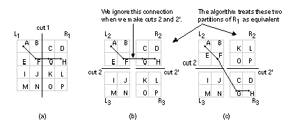
shows a situation in which logic cells G and H are connected to other logic cells (A and F) outside the area R1 that is currently being partitioned. The min-cut algorithm ignores connections outside the area to be divided. Thus logic cells G and H may be placed in partition R3 rather than partition R2. Suggest solutions to this problem.
Hint:
See
Dunlop [1983];
Hartoog [1986]; or the Barnes–Hut galaxy model.
|
|
|
FIGURE 16.33
(For Problem
16.10
.) A problem with the min-cut algorithm is that it ignores connections to logic cells outside the area being partitioned. (a) We perform a vertical cut 1 producing the areas R
1
and R
2
. (b) Next we make a horizontal cut 2, producing L
2
and L
3
, and a cut 2', producing R
2
and R
3
. (c) The min-cut algorithm ignores the connection from L
2
and is equally likely to produce the arrangement shown here when we make cut 2'.
|
16.11 (Benchmarks and statistics, 30 min.) Your boss asks you to compare two placement programs from companies ABC and XYZ. You run five test cases for both on a single netlist, P1. You get results (measured in arbitrary units) of 9, 8, 9, 7, 11 for ABC; 6, 9, 10, 13, 8 for XYZ.
-
a. Calculate the mean and standard deviations for these results.
-
b. What confidence (in the statistical sense) do you have in these figures?
-
c. What can you say about the relative performance of ABC and XYZ?
On average each test case takes about 0.5 hours (wall clock) for both ABC and XYZ. Next you run six test cases on another netlist, P2 with the following results: 4, 6, 7, 8, 5, 7 for ABC, and 4, 5, 3, 6, 4, 3 for XYZ. These test cases take about 0.75 hours (wall clock) each.
-
d. What can you say about the P2 results?
-
e. Given the P1 and P2 results together, what can you say about ABC and XYZ?
-
f. How many P1 test cases should you run to get a result so that you can say ABC is better or worse than XYZ with 90 percent confidence (i.e., you make the right decision 9 out of 10 times)? How long would this take?
-
g. Find the same figures for the P2 netlist. Comment on your answers.
-
h. Suppose you had more netlists and information about the variation of results from each netlist, together with the average time to run each netlist. How would you use this information to get the most meaningful result in the shortest time?
16.12
(Linear and quadratic placement, 20 min.) [
Sigl, Doll, and Johannes, 1991]
Figure 16.34
(a) shows a simple network that we will place.
Figure 16.34
(b) shows the problem. The logic cells are all the same size: 1 grid unit wide by 1 grid unit high. Logic cells 1 and 3 are fixed at the locations shown. Logic cell 2 is movable and placed at coordinates (for the lower-left corner) of (
x
2
, y
2
). The lower-left corners of logic cells should be placed at grid locations and should not overlap.
-
a. What is the connection matrix
c
ij
for this network?
-
b. Calculate and draw (showing the logic-cell coordinates) the placement that minimizes the linear cost function (or objective function)
f
L
,
|
|
|
1
|
n
|
|
|
|
|
f
L
|
=
|
––
|
S
|
c
ij
d
ij
|
|
(16.23)
|
|
|
|
2
|
j
= 1
|
|
|
|
where
d
ij
is the distance between logic cells
i
and
j
.
|

|
|
FIGURE 16.34
Problem
16.12
illustrates placement objectives. (a) An example network for placement. (b) The placement restrictions. Logic cells 1 and 3 are fixed in position, the placement problem is to optimize the position of logic cell 2 under different placement objectives.
|
-
c. Calculate and draw (showing coordinates) the placement that minimizes the quadratic cost function
f
Q
,
|
|
|
1
|
n
|
|
|
|
|
f
Q
|
=
|
––
|
S
|
c
ij
d
ij
2
|
|
(16.24)
|
|
|
|
2
|
j
= 1
|
|
|
|
16.13
(Placement interconnect lengths, 45 min.)
Figure 16.30
(d) shows the actual routing corresponding to a placement with an estimated routing length of 8 units (
Figure 16.30
b).
-
a. Draw the layout (with routing) corresponding to the placement of
Figure 16.30
(c), which has a lower estimated total routing length of 7 units.
-
b. Compare the actual total routing length for both layouts and explain why they are different from the estimated lengths and describe the sources of the errors.
-
c. Consider flipping both logic cells A and B about the
y
-axis in the layout shown in
Figure 16.30
(d). How much does this shorten the total interconnect length? Some placement algorithms consider such moves.
16.14
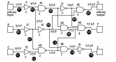
(Zero-slack algorithm, 60 min.) For the circuit of
Figure 16.35
:
-
a. Find all of the arrival, required, and slack times (all delays are in nanoseconds).
|

|
|
FIGURE 16.35
A circuit to illustrate the zero-slack algorithm (Problem
16.14
).
|
-
b. What is the critical path?
-
c. If the gate delay of A2 is increased to 5 ns, what is the new critical path?
-
d. ** Using your answer to part a find the upper bounds on net delays by means of the zero-slack algorithm as follows:
i. Find arrival, required, and slack times on all nets.
ii. Find an input pin
p
with the least nonzero slack
S
p
on a net which has not already been selected. If there are none go to step 6.
ii. Find the path through
p
(may include several gates) on which all pins have slack
S
p
.
iv. Distribute a delay equal to the slack
S
p
along the path assigning a fraction to each net at the output pins of the gates on the path.
v. Work backward from
p
updating all the required times as necessary and forward from
p
updating all the arrival times.
vi. Convert net delays to net lengths.
Hint:
You can consult the original description of the zero-slack algorithm if this is not clear [
Hauge et al., 1987].
16.15
(World planning, 60 min.) The seven continents are (with areas in millions of square miles): Europe—strictly a peninsula of Asia (4.1), Asia (17.2), North America (9.4), South America (6.9), Australia (3.0), Africa (11.7), and Antarctica (5.1). Assume the continents are flexible blocks whose aspect ratio may be adjusted.
-
a. Create a slicing floorplan of the world with a square aspect ratio.
-
b. Draw a world connectivity graph with seven nodes and whose edges are labeled with the distances between Moscow, Beijing, Chicago, Rio de Janeiro, Sydney, Nairobi, and the South Pole.
-
c. Suppose you want to floorplan the world so that the difference in distances between the centers of the continental blocks and the corresponding edges in the world connectivity graph is minimized. How would you measure the differences in distance? Suggest a method to minimize your measure.
-
d. Use an eigenvalue method to floorplan the world. Draw the result with coordinates for each block and explain your approach.
[ Chapter start ] [ Previous page ] [ Next page ] | 


